PCA9535CD,112 NXP Semiconductors, PCA9535CD,112 Datasheet - Page 14
PCA9535CD,112
Manufacturer Part Number
PCA9535CD,112
Description
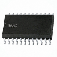
IC I/O EXPANDER I2C 16B 24SOIC
Manufacturer
NXP Semiconductors
Datasheet
1.PCA9535HF118.pdf
(31 pages)
Specifications of PCA9535CD,112
Interface
I²C, SMBus
Number Of I /o
16
Interrupt Output
Yes
Frequency - Clock
400kHz
Voltage - Supply
2.3 V ~ 5.5 V
Operating Temperature
-40°C ~ 85°C
Mounting Type
Surface Mount
Package / Case
24-SOIC (7.5mm Width)
Includes
POR
Lead Free Status / RoHS Status
Lead free / RoHS Compliant
Other names
935285271112
PCA9535CD
PCA9535CD
PCA9535CD
PCA9535CD
Available stocks
Company
Part Number
Manufacturer
Quantity
Price

Part Number:
PCA9535CD,112
Manufacturer:
NXP/恩智浦
Quantity:
20 000


NXP Semiconductors
7. Characteristics of the I
PCA9535_PCA9535C_5
Product data sheet
6.5.3 Interrupt output
7.1.1 START and STOP conditions
7.1 Bit transfer
The open-drain interrupt output is activated when one of the port pins change state and
the pin is configured as an input. The interrupt is deactivated when the input returns to its
previous state or the Input Port register is read (see
output cannot cause an interrupt. Since each 8-bit port is read independently, the interrupt
caused by Port 0 will not be cleared by a read of Port 1 or the other way around.
Remark: Changing an I/O from an output to an input may cause a false interrupt to occur
if the state of the pin does not match the contents of the Input Port register.
The I
lines are a serial data line (SDA) and a serial clock line (SCL). Both lines must be
connected to a positive supply via a pull-up resistor when connected to the output stages
of a device. Data transfer may be initiated only when the bus is not busy.
One data bit is transferred during each clock pulse. The data on the SDA line must remain
stable during the HIGH period of the clock pulse as changes in the data line at this time
will be interpreted as control signals (see
Both data and clock lines remain HIGH when the bus is not busy. A HIGH-to-LOW
transition of the data line while the clock is HIGH is defined as the START condition (S). A
LOW-to-HIGH transition of the data line while the clock is HIGH is defined as the STOP
condition (P) (see
Fig 13. Bit transfer
Fig 14. Definition of START and STOP conditions
2
C-bus is for 2-way, 2-line communication between different ICs or modules. The two
SDA
SCL
START condition
2
SDA
SCL
Figure
C-bus
S
Rev. 05 — 15 September 2008
14).
16-bit I
2
C-bus and SMBus, low power I/O port with interrupt
data valid
data line
stable;
Figure
PCA9535; PCA9535C
allowed
change
of data
13).
Figure
11). A pin configured as an
STOP condition
mba607
P
© NXP B.V. 2008. All rights reserved.
mba608
SDA
SCL
14 of 31
Related parts for PCA9535CD,112
Image
Part Number
Description
Manufacturer
Datasheet
Request
R

Part Number:
Description:
NXP Semiconductors designed the LPC2420/2460 microcontroller around a 16-bit/32-bitARM7TDMI-S CPU core with real-time debug interfaces that include both JTAG andembedded trace
Manufacturer:
NXP Semiconductors
Datasheet:

Part Number:
Description:
NXP Semiconductors designed the LPC2458 microcontroller around a 16-bit/32-bitARM7TDMI-S CPU core with real-time debug interfaces that include both JTAG andembedded trace
Manufacturer:
NXP Semiconductors
Datasheet:
Part Number:
Description:
NXP Semiconductors designed the LPC2468 microcontroller around a 16-bit/32-bitARM7TDMI-S CPU core with real-time debug interfaces that include both JTAG andembedded trace
Manufacturer:
NXP Semiconductors
Datasheet:
Part Number:
Description:
NXP Semiconductors designed the LPC2470 microcontroller, powered by theARM7TDMI-S core, to be a highly integrated microcontroller for a wide range ofapplications that require advanced communications and high quality graphic displays
Manufacturer:
NXP Semiconductors
Datasheet:
Part Number:
Description:
NXP Semiconductors designed the LPC2478 microcontroller, powered by theARM7TDMI-S core, to be a highly integrated microcontroller for a wide range ofapplications that require advanced communications and high quality graphic displays
Manufacturer:
NXP Semiconductors
Datasheet:
Part Number:
Description:
The Philips Semiconductors XA (eXtended Architecture) family of 16-bit single-chip microcontrollers is powerful enough to easily handle the requirements of high performance embedded applications, yet inexpensive enough to compete in the market for hi
Manufacturer:
NXP Semiconductors
Datasheet:
Part Number:
Description:
The XA-S3 device is a member of Philips Semiconductors? XA(eXtended Architecture) family of high performance 16-bitsingle-chip microcontrollers
Manufacturer:
NXP Semiconductors
Datasheet:

Part Number:
Description:
The NXP BlueStreak LH75401/LH75411 family consists of two low-cost 16/32-bit System-on-Chip (SoC) devices
Manufacturer:
NXP Semiconductors
Datasheet:
Part Number:
Description:
The NXP LPC3130/3131 combine an 180 MHz ARM926EJ-S CPU core, high-speed USB2
Manufacturer:
NXP Semiconductors
Datasheet:
Part Number:
Description:
The NXP LPC3141 combine a 270 MHz ARM926EJ-S CPU core, High-speed USB 2
Manufacturer:
NXP Semiconductors
Part Number:
Description:
The NXP LPC3143 combine a 270 MHz ARM926EJ-S CPU core, High-speed USB 2
Manufacturer:
NXP Semiconductors

Part Number:
Description:
The NXP LPC3152 combines an 180 MHz ARM926EJ-S CPU core, High-speed USB 2
Manufacturer:
NXP Semiconductors
Part Number:
Description:
The NXP LPC3154 combines an 180 MHz ARM926EJ-S CPU core, High-speed USB 2
Manufacturer:
NXP Semiconductors

Part Number:
Description:
Standard level N-channel enhancement mode Field-Effect Transistor (FET) in a plastic package using NXP High-Performance Automotive (HPA) TrenchMOS technology
Manufacturer:
NXP Semiconductors
Datasheet: