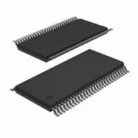
PCA9506DGG,518 NXP Semiconductors, PCA9506DGG,518 Datasheet - Page 7

PCA9506DGG,518
Manufacturer Part Number
PCA9506DGG,518
Description
IC I/O EXPANDER I2C 40B 56TSSOP
Manufacturer
NXP Semiconductors
Specifications of PCA9506DGG,518
Package / Case
56-TSSOP
Interface
I²C
Number Of I /o
40
Interrupt Output
Yes
Frequency - Clock
400kHz
Voltage - Supply
2.3 V ~ 5.5 V
Operating Temperature
-40°C ~ 85°C
Mounting Type
Surface Mount
Includes
POR
Logic Family
PCA9506
Number Of Lines (input / Output)
40.0 / 40.0
Operating Supply Voltage
2.3 V to 5.5 V
Power Dissipation
500 mW
Operating Temperature Range
- 40 C to + 85 C
Input Voltage
5.5 V
Logic Type
I/O Expander
Maximum Clock Frequency
400 KHz
Mounting Style
SMD/SMT
Number Of Input Lines
40.0
Number Of Output Lines
40.0
Output Current
50 mA
Output Voltage
5.5 V
Operating Temperature (min)
-40C
Operating Temperature Classification
Industrial
Operating Temperature (max)
85C
Package Type
TSSOP
Rad Hardened
No
Lead Free Status / RoHS Status
Lead free / RoHS Compliant
Lead Free Status / RoHS Status
Lead free / RoHS Compliant, Lead free / RoHS Compliant
Other names
935280798518
PCA9506DGG-T
PCA9506DGG-T
PCA9506DGG-T
PCA9506DGG-T
Philips Semiconductors
7. Functional description
9397 750 14939
Product data sheet
7.1 Device address
7.2 Command register
Table 2:
[1]
Refer to
IO0_0 to
Following a START condition, the bus master must send the address of the slave it is
accessing and the operation it wants to perform (read or write). The address of the
PCA9506 is shown in
addresses and need to be connected to V
pull-up resistors are incorporated on A2, A1, and A0.
The last bit of the first byte defines the operation to be performed. When set to logic 1 a
read is selected, while a logic 0 selects a write operation.
Following the successful acknowledgement of the slave address + R/W bit, the bus master
will send a byte to the PCA9506, which will be stored in the Command register.
Symbol
OE
INT
RESET
Fig 5. PCA9506 address
Fig 6. Command register
HVQFN package die supply ground is connected to both V
be connected to supply ground for proper device operation. For enhanced thermal, electrical, and board
level performance, the exposed pad needs to be soldered to the board using a corresponding thermal pad
on the board and for proper heat conduction through the board, thermal vias need to be incorporated in the
printed-circuit board in the thermal pad region.
Figure 1 “Block diagram of PCA9506”
IO4_7”.
Pin description
Pin
TSSOP56
30
55
56
Rev. 01 — 14 February 2006
Figure
AI
Auto-Increment
1
…continued
0
5. Slave address pins A2, A1, and A0 choose 1 of 8 slave
0
D5
0
HVQFN56
23
48
49
1
D4
fixed
0
register number
slave address
0
D3
40-bit I
0
DD
0
D2
0
(1) or V
programmable
A2
002aab495
2
D1
and
0
C-bus I/O port with RESET, OE, and INT
A1
D0
Type
I
O
I
SS
0
Figure 2 “Simplified schematic of
SS
002aab494
pins and exposed center pad. V
A0 R/W
default at power-up
or after RESET
(0). To conserve power, no internal
© Koninklijke Philips Electronics N.V. 2006. All rights reserved.
Description
active LOW output enable input
active LOW interrupt output
active LOW reset input
PCA9506
SS
pins must
7 of 30


