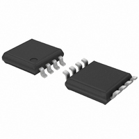
PCA9510ADP,118 NXP Semiconductors, PCA9510ADP,118 Datasheet - Page 4

PCA9510ADP,118
Manufacturer Part Number
PCA9510ADP,118
Description
IC I2C/SMBUS BUFF 8TSSOP
Manufacturer
NXP Semiconductors
Type
Bufferr
Datasheet
1.PCA9510ADP118.pdf
(24 pages)
Specifications of PCA9510ADP,118
Package / Case
8-TSSOP
Tx/rx Type
I²C Logic
Delay Time
35ns
Capacitance - Input
1.9pF
Voltage - Supply
2.7 V ~ 5.5 V
Current - Supply
6mA
Mounting Type
Surface Mount
Supply Voltage (max)
5.5 V
Supply Voltage (min)
2.7 V
Maximum Operating Temperature
+ 85 C
Mounting Style
SMD/SMT
Minimum Operating Temperature
- 40 C
Lead Free Status / RoHS Status
Lead free / RoHS Compliant
Lead Free Status / RoHS Status
Lead free / RoHS Compliant, Lead free / RoHS Compliant
Other names
568-3358-2
935279844118
PCA9510ADP-T
935279844118
PCA9510ADP-T
NXP Semiconductors
7. Pinning information
PCA9510A_4
Product data sheet
7.1 Pinning
7.2 Pin description
Table 3.
Symbol
ENABLE
SCLOUT
SCLIN
GND
READY
SDAIN
SDAOUT
V
Fig 2.
CC
SCLOUT
ENABLE
SCLIN
GND
Pin configuration for SO8
Pin description
Pin
1
2
3
4
5
6
7
8
1
2
3
4
PCA9510AD
Description
Chip enable. Grounding this input puts the part in a Low current (< 1 A)
mode. It also disables the rise time accelerators, isolates SDAIN from
SDAOUT and isolates SCLIN from SCLOUT.
serial clock output to and from the SCL bus on the card
serial clock input to and from the SCL bus on the backplane
ground supply; connect this pin to a ground plane for best results
open-drain output which pulls LOW when SDAIN and SCLIN are
disconnected from SDAOUT and SCLOUT, and goes HIGH when the two
sides are connected
serial data input to and from the SDA bus on the backplane
serial data output to and from the SDA bus on the card
power supply
002aab782
Rev. 04 — 18 August 2009
8
7
6
5
V
SDAOUT
SDAIN
READY
CC
Hot swappable I
Fig 3.
SCLOUT
ENABLE
SCLIN
GND
Pin configuration for TSSOP8
2
1
2
3
4
C-bus and SMBus bus buffer
PCA9510ADP
PCA9510A
002aab783
© NXP B.V. 2009. All rights reserved.
8
7
6
5
V
SDAOUT
SDAIN
READY
CC
4 of 24


