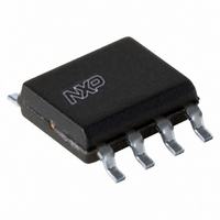
PCA9509D,118 NXP Semiconductors, PCA9509D,118 Datasheet - Page 5

PCA9509D,118
Manufacturer Part Number
PCA9509D,118
Description
IC REPEAT I2C/SMBUS 8-SOIC
Manufacturer
NXP Semiconductors
Type
Repeaterr
Datasheet
1.PCA9509DP118.pdf
(19 pages)
Specifications of PCA9509D,118
Package / Case
8-SOIC (3.9mm Width)
Tx/rx Type
I²C Logic
Delay Time
109ns
Capacitance - Input
2pF
Voltage - Supply
3 V ~ 5.5 V
Current - Supply
5mA
Mounting Type
Surface Mount
Logic Family
PCA9509
Operating Supply Voltage
1 V to 5.5 V
Power Dissipation
100 mW
Operating Temperature Range
- 40 C to + 85 C
Input Voltage
5 V
Logic Type
I2C Bus
Maximum Clock Frequency
400 KHz
Mounting Style
SMD/SMT
Output Current
20 mA
Output Voltage
5 V
Lead Free Status / RoHS Status
Lead free / RoHS Compliant
Lead Free Status / RoHS Status
Lead free / RoHS Compliant, Lead free / RoHS Compliant
Other names
935282227118
PCA9509D-T
PCA9509D-T
PCA9509D-T
PCA9509D-T
NXP Semiconductors
7. Application design-in information
PCA9509_5
Product data sheet
6.2 I
As with the standard I
HIGH levels on the buffered bus (standard open-collector configuration of the I
The size of these pull-up resistors depends on the system. Each of the port A I/Os has an
internal pull-up current source and does not require the external pull-up resistor. Port B is
designed to work with Standard-mode and Fast-mode I
SMBus devices. Standard-mode I
limits the termination current to 3 mA in a generic I
devices and multiple masters are possible. Under certain conditions higher termination
currents can be used.
A typical application is shown in
I
devices can be placed on either bus.
When port B of the PCA9509 is pulled LOW by a driver on the I
hysteresis detects the falling edge when it goes below 0.3V
driver on port A to turn on, causing port A to pull down to about 0.2 V. When port A of the
PCA9509 falls, first a comparator detects the falling edge and causes the internal driver
on port B to turn on and pull the port B pin down to ground. In order to illustrate what
would be seen in a typical application, refer to
Figure 5
would be observed on the B bus. This looks like a normal I
On the A bus side of the PCA9509, the clock and data lines would have a positive offset
from ground equal to the V
be pulled to the V
the end of the acknowledge, the level rises only to the LOW level set by the driver in the
PCA9509 for a short delay while the B bus side rises above 0.5V
HIGH. It is important to note that any arbitration or clock stretching events require that the
LOW level on the A bus side at the input of the PCA9509 (V
recognized by the PCA9509 and then transmitted to the B bus side.
2
2
Fig 5.
C-bus while the master is connected to a 3.3 V bus. Both buses run at 400 kHz. Master
C-bus systems
were to write to the slave through the PCA9509, waveforms shown in
Typical application
OL
MASTER
CPU
of the master device, which is very close to ground in this example. At
2
SDA
SCL
C-bus system, pull-up resistors are required to provide the logic
Rev. 05 — 10 July 2009
OL
10 k
bus A
1.1 V
of the PCA9509. After the 8
1.1 V
Figure
2
C-bus devices only specify 3 mA output drive; this
A1
A2
EN
V
5. In this example, the CPU is running on a 1.1 V
CC(A)
PCA9509
Level translating I
Figure 6
V
CC(B)
2
B1
B2
C-bus system where Standard-mode
10 k
2
and
C-bus devices in addition to
bus B
th
3.3 V
2
CC(B)
C-bus transmission.
clock pulse, the data line will
Figure
IL
10 k
) is below V
2
SDA
SCL
2
C-bus, a CMOS
and causes the internal
CC(B)
C-bus/SMBus repeater
400 kHz
SLAVE
002aac128
7. If the bus master in
, then it continues
PCA9509
© NXP B.V. 2009. All rights reserved.
ILc
to be
2
Figure 6
C-bus).
5 of 19


