SCANSTA101SM/NOPB National Semiconductor, SCANSTA101SM/NOPB Datasheet - Page 3
SCANSTA101SM/NOPB
Manufacturer Part Number
SCANSTA101SM/NOPB
Description
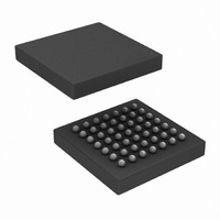
IC TEST MASTER LOW-VOLT 49FBGA
Manufacturer
National Semiconductor
Datasheet
1.SCANSTA101SMNOPB.pdf
(32 pages)
Specifications of SCANSTA101SM/NOPB
Applications
Testing Equipment
Interface
IEEE 1149.1
Voltage - Supply
3 V ~ 3.6 V
Package / Case
49-FBGA
Mounting Type
Surface Mount
Lead Free Status / RoHS Status
Lead free / RoHS Compliant
Other names
*SCANSTA101SM
*SCANSTA101SM/NOPB
SCANSTA101SM
*SCANSTA101SM/NOPB
SCANSTA101SM
Available stocks
Company
Part Number
Manufacturer
Quantity
Price
Company:

Part Number:
SCANSTA101SM/NOPB
Manufacturer:
Texas Instruments
Quantity:
10 000


VCC
GND
D(15:0)
D(31:16)
(Note
A(4:0)
SCK
INT
OE
DTACK
R/W
STB
CE
RST
TDO
TDI
TMS
TCK
TRST
TDI_SM
TDO_SM
TMS_SM
TCK_SM
TRST0_SM
TRST1_SM
(Note
TRIST_SM
TABLE 2. Pin Descriptions
Note 1: D(31:16) in the Parallel Processor Interface and TRST1_SM in the Serial Scan Interface are not bonded out for the packaged device. These are used in
the 32-bit IP Macro Mode only.
1)
1)
Name
Pin
No. Pins
16
16
4
4
5
1
1
1
1
1
1
1
1
1
1
1
1
1
1
1
1
1
1
1
1
N/A
N/A
I/O
I/O
I/O
O
O
O
O
O
O
O
O
O
I
I
I
I
I
I
I
I
I
I
I
I
Power
Ground
Bidirectional Data Bus. Signals are bonded out for the packaged
device.
Bidirectional Data Bus. These signals are not available in the
packaged device.
Address Bus
The system clock that drives all internal timing. TCK_SM is a gated,
divided and buffered version of SCK.
Interrupt Output
Output enable that will TRI-STATE all 1149.1 "_SM" outputs when
high.
DTACK is used to synchronize asynchronous transfers between the
host and the SCANSTA101. When CE is high, DTACK is tristated.
When CE is low, DTACK is enabled. DTACK goes low when data has
been registered and then goes TRI-STATE
completed.
R/W defines a PPI cycle. Read when high, write when low.
Strobe is used for timing all PPI transfers. D(15:0), or D(31:0) in 32-
bit mode
setup is with respect to the falling edge of STB and data valid hold is
with respect to rising edge of STB.
Chip Enable, when low, enables the PPI for data transfers. CE can
remain low during back-to-back accesses. D(15:0), or D(31:0) in 32-
bit
Asynchronous reset, when low, initializes the SCANSTA101.
Test Data Out is the serial scan output from the SCANSTA101. TDO
is enabled when OE is low.
Test Data In is the serial scan input to the SCANSTA101.
Test Mode Select. The Test Mode Select pin is a serial input used to
accept control logic to the test & debug interface.
Test Clock Input for 1149.1
Test Reset. This pin should be tied to ground by a 1K resistor to hold
the Test and Debug Interface in the Test-Logic-Reset state during
device power-up. This avoids invalid states when ramping supply
voltages.
STA Master Test Data Input in the Serial Scan Interface
STA Master Test Data Output in the Serial Scan Interface
STA Master Test Mode Select in the Serial Scan Interface
STA Master Test Clock in the Serial Scan Interface
STA Master Test Reset output in the Serial Scan Interface
Redundant ScanMaster TRST. This signal is not available for the
packaged device.
The TRI-STATE notification pin exerts a high signal when TDO_SM
is at TRI-STATE
3
mode(Note
(Note
1), and DTACK are tristated when CE is high.
1), are at TRI-STATE when STB is high. Data valid
Description
®
when the cycle has
www.national.com
Related parts for SCANSTA101SM/NOPB
Image
Part Number
Description
Manufacturer
Datasheet
Request
R

Part Number:
Description:
Low Voltage Ieee 1149.1 Sta Master
Manufacturer:
National Semiconductor Corporation
Datasheet:

Part Number:
Description:
National Semiconductor [8-Bit D/A Converter]
Manufacturer:
National Semiconductor
Datasheet:
Part Number:
Description:
National Semiconductor [Media Coprocessor]
Manufacturer:
National Semiconductor
Datasheet:
Part Number:
Description:
Digitally Controlled Tone and Volume Circuit with Stereo Audio Power Amplifier, Microphone Preamp Stage and National 3D Sound
Manufacturer:
National Semiconductor
Datasheet:
Part Number:
Description:
Digitally Controlled Tone and Volume Circuit with Stereo Audio Power Amplifier, Microphone Preamp Stage and National 3D Sound
Manufacturer:
National Semiconductor
Datasheet:
Part Number:
Description:
AC97 Rev 2 Codec with Sample Rate Conversion and National 3D Sound
Manufacturer:
National Semiconductor
Part Number:
Description:
Manufacturer:
National Semiconductor
Datasheet:
Part Number:
Description:
Manufacturer:
National Semiconductor
Datasheet:
Part Number:
Description:
General Purpose, Low Voltage, Low Power, Rail-to-Rail Output Operational Amplifiers
Manufacturer:
National Semiconductor
Datasheet:
Part Number:
Description:
8-bit 20 MSPS flash A/D converter.
Manufacturer:
National Semiconductor
Datasheet:
Part Number:
Description:
Low Noise Quad Operational Amplifier
Manufacturer:
National Semiconductor
Datasheet:
Part Number:
Description:
Quad Differential Line Receivers
Manufacturer:
National Semiconductor
Datasheet:
Part Number:
Description:
Quad High Speed Trapezoidal? Bus Transceiver
Manufacturer:
National Semiconductor
Datasheet:
Part Number:
Description:
Dual Line Receiver
Manufacturer:
National Semiconductor
Datasheet: