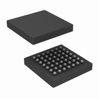
SCANSTA101SM/NOPB National Semiconductor, SCANSTA101SM/NOPB Datasheet - Page 5

SCANSTA101SM/NOPB
Manufacturer Part Number
SCANSTA101SM/NOPB
Description
IC TEST MASTER LOW-VOLT 49FBGA
Manufacturer
National Semiconductor
Datasheet
1.SCANSTA101SMNOPB.pdf
(32 pages)
Specifications of SCANSTA101SM/NOPB
Applications
Testing Equipment
Interface
IEEE 1149.1
Voltage - Supply
3 V ~ 3.6 V
Package / Case
49-FBGA
Mounting Type
Surface Mount
Lead Free Status / RoHS Status
Lead free / RoHS Compliant
Other names
*SCANSTA101SM
*SCANSTA101SM/NOPB
SCANSTA101SM
*SCANSTA101SM/NOPB
SCANSTA101SM
Available stocks
Company
Part Number
Manufacturer
Quantity
Price
Company:
Part Number:
SCANSTA101SM/NOPB
Manufacturer:
Texas Instruments
Quantity:
10 000
PARALLEL PROCESSOR INTERFACE (PPI)
t
t
t
t
t
t
t
t
t
t
t
t
t
t
t
t
t
S1
H1
D1
D1
D1
D1
D1
D1
D2
D2
D2
D2
D2
D2
D3
pHL1
W
Symbol
AC Electrical Characteristics/Operating Requirements
Over recommended operating supply voltage and temperature ranges unless otherwise specified. C
otherwise specified.
Set Up Time
CE, R/W, Addr, Data to STB
Hold Time
CE, R/W, Addr, Data to DTACK
Propagation Delay
STB low to DTACK low, Register Write
Propagation Delay
STB low to DTACK low, Register Read
Propagation Delay
STB low to DTACK low, Memory Write:
16-bit first access
Propagation Delay
STB low to DTACK low, Memory Write:
16-bit second access
Propagation Delay
STB low to DTACK low, Memory Read:
16-bit first access
Propagation Delay
STB low to DTACK low, Memory Read:
16-bit second access
Propagation Delay
STB high to DTACK TRISTATE,
Register Write
Propagation Delay
STB high to DTACK TRISTATE,
Register Read
Propagation Delay
STB high to DTACK TRISTATE,
Memory Write: 16-bit first access
Propagation Delay
STB high to DTACK TRISTATE,
Memory Write: 16-bit second access
Propagation Delay
STB high to DTACK TRISTATE,
Memory Read: 16-bit first access
Propagation Delay
STB high to DTACK TRISTATE,
Memory Read: 16-bit second access
Propagation Delay
Output data valid to DTACK low, all read
cycles
Propagation Delay
STB low to INT low, register write (clears
Interrupt)
Clock Pulse Width, SCK, H or L
Parameter
Figures 11, 12
Figures 11, 12
Figure 11
Figure 12
Figure 11
Figure 11
Figure 12
Figure 12
Figure 11
Figure 12
Figure 11
Figure 11
Figure 12
Figure 12
Figure 12
Figure 11
Conditions
5
(Note
# of SCK
9 or 10
2 or 3
4 or 5
3 or 4
7 or 8
3 or 4
1 or 2
1 or 2
1 or 2
1 or 2
1 or 2
1 or 2
5 or 6
3,
1
Note
4)
L
= 50 pF, R
Min
3.0
0
0
L
= 500Ω unless
Max
11.5
11.5
11.5
11.5
11.5
11.5
10.0
10.0
10.0
10.0
10.0
10.0
10.5
www.national.com
Units
ns
ns
ns
ns
ns
ns
ns
ns
ns
ns
ns
ns
ns
ns
ns
ns
ns


