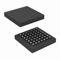
SCANSTA101SM/NOPB National Semiconductor, SCANSTA101SM/NOPB Datasheet - Page 30

SCANSTA101SM/NOPB
Manufacturer Part Number
SCANSTA101SM/NOPB
Description
IC TEST MASTER LOW-VOLT 49FBGA
Manufacturer
National Semiconductor
Datasheet
1.SCANSTA101SMNOPB.pdf
(32 pages)
Specifications of SCANSTA101SM/NOPB
Applications
Testing Equipment
Interface
IEEE 1149.1
Voltage - Supply
3 V ~ 3.6 V
Package / Case
49-FBGA
Mounting Type
Surface Mount
Lead Free Status / RoHS Status
Lead free / RoHS Compliant
Other names
*SCANSTA101SM
*SCANSTA101SM/NOPB
SCANSTA101SM
*SCANSTA101SM/NOPB
SCANSTA101SM
Available stocks
Company
Part Number
Manufacturer
Quantity
Price
Company:
Part Number:
SCANSTA101SM/NOPB
Manufacturer:
Texas Instruments
Quantity:
10 000
www.national.com
Instruction Mnemonic
EXTEST
SAMPLE/PRELOAD
BYPASS
IDCODE
HIGHZ
CLAMP
RUNBIST
SCANTEST
BSR
Testability Details - IEEE 1149.1 Support
Bit#
BIST SUPPORT
The memory BIST can be initiated through JTAG interface
using the RUNBIST instruction or by setting the Onboard
Memory BIST bit in the Start register. When the memory BIST
is initiated through the JTAG interface the result of pass/fail
will be set in the Memory BIST Result bit in the Status register
and also in the BIST status register that can be accessed
through the JTAG interface. The BIST status register is a one
bit register and is connected in the serial path of TDO and TDI
Revision History
January, 2010 – Applications information updates and clari-
fication. No specification changes.
0
1
2
3
4
5
6
7
8
9
Version
"0000"
Signal Name
ADDRESS[4]
ADDRESS[3]
ADDRESS[2]
ADDRESS[1]
ADDRESS[0]
SCK
RST
R/W
STB
CE
"1111 1100 0001 0111"
Binary Instruction Code
000
001
111
010
011
100
110
101
BSR
Bit#
10
11
12
13
14
15
16
17
18
19
Part Number
TABLE 35. Supported IEEE 1149.1 Instruction Set
TABLE 37. Boundary Scan Register Definition
TABLE 36. IDCODE Register Description
Signal Name
DATA[15]
DATA[14]
DATA[13]
DATA[12]
DATA[11]
DATA[10]
DATA[9]
DATA[8]
DTACK
INT
Description
Allows off-chip circuitry and interconnect to be tested.
Allows snapshot of normal operation. Also allows data to be loaded
on parallel output boundary scan registers.
Places device in bypass mode so that there is single shift register
stage between TDI and TDO.
Allows scanning of the device identification register.
Will TRI-STATE all output drivers with the exception of TDO.
Allows the state of the signals driven from component pins to be
determined from the boundary-scan register while the BYPASS
register is selected as the serial path between TDI and TDO.
Enables on chip BIST logic to perform memory BIST.
Allows the assertion of internal test_mode signal to prevent the
asynchronous resets from inadvertently resetting the flip-flops during
internal scan. Used in factory test.
30
BSR
Bit#
20
21
22
23
24
25
26
27
28
29
when the RUNBIST instruction is scanned into the instruction
register. Once the BIST is done, the contents of the BIST sta-
tus register can be scanned out to determine whether the
memory BIST passed or failed. If the memory BIST is initiated
through the Onboard Memory BIST bit in the Start register the
result of pass/fail will be set only in the BIST Result bit in the
status register. The memory BIST will initialize the memory to
zero.
Signal Name
TDO_SM
TMS_SM
DATA[7]
DATA[6]
DATA[5]
DATA[4]
DATA[3]
DATA[2]
DATA[1]
DATA[0]
Manufacturer Identity
"000 0000 1111"
BSR
Bit#
30
31
32
33
34
Signal Name
TRST0_SM
TCK_SM
TDI_SM
TRIST
OE
Start Bit
"1"


