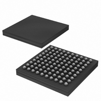
DS33ZH11+ Maxim Integrated Products, DS33ZH11+ Datasheet - Page 26

DS33ZH11+
Manufacturer Part Number
DS33ZH11+
Description
IC MAPPER ETHERNET 100CSBGA
Manufacturer
Maxim Integrated Products
Datasheet
1.DS33Z11.pdf
(172 pages)
Specifications of DS33ZH11+
Applications
Data Transport
Interface
Serial
Voltage - Supply
1.8V, 2.5V, 3.3V
Package / Case
100-LBGA
Mounting Type
Surface Mount
Lead Free Status / RoHS Status
Lead free / RoHS Compliant
- Current page: 26 of 172
- Download datasheet (2Mb)
JTCLK
NAME
JTRST
JTDO
JTMS
V
V
JTDI
V
DD3.3
DD1.8
SS
E11, E12,
F12, F13,
DS33Z11
G5–G10,
D12, E3,
A12, D1,
K9, K10,
F4, F10,
H5–H10
L3, L12,
J5–J11,
D2, D3,
E7, E8,
K3, K5,
K7, K8,
F8, F9,
J4, K4,
CSBGA
PIN #
M13
(169)
K12
E6
D4
E5
E4
F7
DS33ZH1
F10, H2,
D8, H10
BGA(100)
A7, D4–
A1, F6,
A5, B4,
E4–E7
PIN #
J10
—
—
—
—
—
1
TYPE
POWER SUPPLIES
JTAG INTERFACE
Ipu
Ipu
Ipu
Ipu
Oz
I
I
I
26 of 172
Active-Low JTAG Reset: JTRST is used to
asynchronously reset the test access port controller. After
power-up, a rising edge on JTRST will reset the test port
and cause the device IO enter the JTAG DEVICE ID
mode. Pulling JTRST low restores normal device
operation. JTRST is pulled HIGH internally via a 10kΩ
resistor operation. If boundary scan is not used, this pin
should be held low.
JTAG Clock: This signal is used to shift data into JTDI on
the rising edge and out of JTDO on the falling edge.
JTAG Data Out: Test instructions and data are clocked
out of this pin on the falling edge of JTCLK. If not used,
this pin should be left unconnected.
JTAG Data In: Test instructions and data are clocked into
this pin on the rising edge of JTCLK. This pin has a 10kΩ
pullup resistor.
JTAG Mode Select: This pin is sampled on the rising
edge of JTCLK and is used to place the test access port
into the various defined IEEE 1149.1 states. This pin has
a 10kΩ pullup resistor.
Connect to 3.3V Power Supply
Connect to 1.8V Power Supply
Connect to the Common Supply Ground
FUNCTION
Related parts for DS33ZH11+
Image
Part Number
Description
Manufacturer
Datasheet
Request
R

Part Number:
Description:
MAX7528KCWPMaxim Integrated Products [CMOS Dual 8-Bit Buffered Multiplying DACs]
Manufacturer:
Maxim Integrated Products
Datasheet:

Part Number:
Description:
Single +5V, fully integrated, 1.25Gbps laser diode driver.
Manufacturer:
Maxim Integrated Products
Datasheet:

Part Number:
Description:
Single +5V, fully integrated, 155Mbps laser diode driver.
Manufacturer:
Maxim Integrated Products
Datasheet:

Part Number:
Description:
VRD11/VRD10, K8 Rev F 2/3/4-Phase PWM Controllers with Integrated Dual MOSFET Drivers
Manufacturer:
Maxim Integrated Products
Datasheet:

Part Number:
Description:
Highly Integrated Level 2 SMBus Battery Chargers
Manufacturer:
Maxim Integrated Products
Datasheet:

Part Number:
Description:
Current Monitor and Accumulator with Integrated Sense Resistor; ; Temperature Range: -40°C to +85°C
Manufacturer:
Maxim Integrated Products

Part Number:
Description:
TSSOP 14/A�/RS-485 Transceivers with Integrated 100O/120O Termination Resis
Manufacturer:
Maxim Integrated Products

Part Number:
Description:
TSSOP 14/A�/RS-485 Transceivers with Integrated 100O/120O Termination Resis
Manufacturer:
Maxim Integrated Products

Part Number:
Description:
QFN 16/A�/AC-DC and DC-DC Peak-Current-Mode Converters with Integrated Step
Manufacturer:
Maxim Integrated Products

Part Number:
Description:
TDFN/A/65V, 1A, 600KHZ, SYNCHRONOUS STEP-DOWN REGULATOR WITH INTEGRATED SWI
Manufacturer:
Maxim Integrated Products

Part Number:
Description:
Integrated Temperature Controller f
Manufacturer:
Maxim Integrated Products

Part Number:
Description:
SOT23-6/I�/45MHz to 650MHz, Integrated IF VCOs with Differential Output
Manufacturer:
Maxim Integrated Products

Part Number:
Description:
SOT23-6/I�/45MHz to 650MHz, Integrated IF VCOs with Differential Output
Manufacturer:
Maxim Integrated Products

Part Number:
Description:
EVALUATION KIT/2.4GHZ TO 2.5GHZ 802.11G/B RF TRANSCEIVER WITH INTEGRATED PA
Manufacturer:
Maxim Integrated Products

Part Number:
Description:
QFN/E/DUAL PCIE/SATA HIGH SPEED SWITCH WITH INTEGRATED BIAS RESISTOR
Manufacturer:
Maxim Integrated Products
Datasheet:


