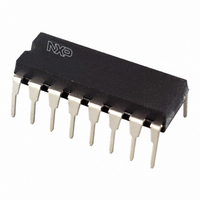
74HC4052N,652 NXP Semiconductors, 74HC4052N,652 Datasheet - Page 16

74HC4052N,652
Manufacturer Part Number
74HC4052N,652
Description
IC MUX/DEMUX DUAL 4X1 16DIP
Manufacturer
NXP Semiconductors
Series
74HCr
Datasheet
1.74HC4052N652.pdf
(28 pages)
Specifications of 74HC4052N,652
Package / Case
16-DIP (0.300", 7.62mm)
Function
Multiplexer/Demultiplexer
Circuit
2 x 4:1
On-state Resistance
60 Ohm
Voltage Supply Source
Dual Supply
Voltage - Supply, Single/dual (±)
±2 V ~ 10 V
Current - Supply
320µA
Operating Temperature
-40°C ~ 125°C
Mounting Type
Through Hole
Number Of Channels
2 Channel
On Resistance (max)
150 Ohm (Typ) @ 2 V
On Time (max)
105 ns (Typ) @ 2 V
Off Time (max)
74 ns (Typ) @ 2 V
Supply Voltage (max)
10 V
Supply Voltage (min)
2 V
Maximum Power Dissipation
500 mW
Maximum Operating Temperature
+ 125 C
Minimum Operating Temperature
- 40 C
Mounting Style
Through Hole
Number Of Switches
Dual
Lead Free Status / RoHS Status
Lead free / RoHS Compliant
Lead Free Status / RoHS Status
Lead free / RoHS Compliant, Lead free / RoHS Compliant
Other names
568-1457-5
74HC4052N
933669750652
74HC4052N
933669750652
Available stocks
Company
Part Number
Manufacturer
Quantity
Price
Company:
Part Number:
74HC4052N,652
Manufacturer:
NXP Semiconductors
Quantity:
1 550
NXP Semiconductors
Table 11.
[1]
[2]
12. Additional dynamic characteristics
Table 12.
Recommended conditions and typical values; GND = 0 V; T
V
V
[1]
[2]
74HC_HCT4052
Product data sheet
Test
t
t
t
Symbol
d
α
Xtalk
V
f
PHL
PZH
PZL
(−3dB)
is
os
sin
iso
ct
is the input voltage at pins nYn or nZ, whichever is assigned as an input.
is the output voltage at pins nYn or nZ, whichever is assigned as an output.
, t
, t
, t
t
V
a) For 74HC4052: V
b) For 74HCT4052: V
Adjust input voltage V
Adjust input voltage V
r
I
PLZ
= t
PLH
PHZ
values:
f
= 6 ns; when measuring f
Test data
Additional dynamic characteristics
Parameter
sine-wave distortion
isolation (OFF-state)
crosstalk
crosstalk voltage
−3 dB frequency response
I
is
is
= V
I
Input
V
[2]
[2]
[2]
= 3 V
to 0 dBm level (0 dBm = 1 mW into 600 Ω).
to 0 dBm level at V
I
CC
max
, there is no constraint to t
V
pulse
V
V
is
CC
EE
All information provided in this document is subject to legal disclaimers.
os
Conditions
f
f
R
between two switches/multiplexers;
R
peak-to-peak value; between control and any
switch; R
wave between V
see
R
for 1 MHz (0 dBm = 1 mW into 50 Ω).
i
i
= 1 kHz; R
= 10 kHz; R
L
L
L
V
V
V
V
V
V
V
V
V
V
V
V
= 600 Ω; f
= 600 Ω; f
= 50 Ω; see
is
is
is
is
CC
CC
CC
CC
CC
CC
CC
CC
Figure 19
= 4.0 V (p-p); V
= 4.0 V (p-p); V
Rev. 7 — 12 January 2011
= 8.0 V (p-p); V
= 8.0 V (p-p); V
= 2.25 V; V
= 4.5 V; V
= 2.25 V; V
= 4.5 V; V
= 4.5 V; V
= 4.5 V; V
= 2.25 V; V
= 4.5 V; V
t
at f
< 2 ns
< 2 ns
< 2 ns
r
L
, t
= 600 Ω; f
max
f
L
i
i
r
L
= 10 kΩ; see
= 1 MHz; see
= 1 MHz; see
and t
amb
= 10 kΩ; see
Figure 20
CC
EE
EE
EE
EE
EE
EE
EE
EE
f
= 25
= −4.5 V
= −4.5 V
and GND; t
= 0 V
= −4.5 V
= −4.5 V
with 50 % duty factor.
i
CC
CC
= −2.25 V
= −2.25 V
= −2.25 V
CC
CC
other
6 ns
6 ns
6 ns
= 1 MHz; E or Sn square
Dual 4-channel analog multiplexer/demultiplexer
= 2.25 V; V
= 2.25 V; V
°
= 4.5 V; V
= 4.5 V; V
C; C
74HC4052; 74HCT4052
[1]
Figure 16
Figure 17
Figure 18
Figure 16
L
r
= 50 pF.
= t
EE
EE
f
EE
EE
Load
C
50 pF
50 pF
50 pF
= 6 ns;
L
= −4.5 V
= −4.5 V
= −2.25 V
= −2.25 V
R
1 kΩ
1 kΩ
1 kΩ
[1]
[1]
[1]
[1]
[2]
[2]
L
Min
-
-
-
-
-
-
-
-
-
-
-
-
Typ
0.04
0.02
0.12
0.06
−50
−50
−60
−60
110
220
170
180
© NXP B.V. 2011. All rights reserved.
S1 position
open
V
V
EE
CC
Max
-
-
-
-
-
-
-
-
-
-
-
-
16 of 28
Unit
%
%
%
%
dB
dB
dB
dB
mV
mV
MHz
MHz


