OM13001,598 NXP Semiconductors, OM13001,598 Datasheet - Page 35
OM13001,598
Manufacturer Part Number
OM13001,598
Description
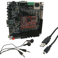
EA LPC177X/8X EVAL BOARD
Manufacturer
NXP Semiconductors
Series
-r
Type
MCUr
Specifications of OM13001,598
Contents
Board, Cable, Headphones, Registration Card
Lead Free Status / Rohs Status
Lead free / RoHS Compliant
For Use With/related Products
LPC1788
Other names
568-6707


NXP Semiconductors
Table 3.
Not all functions are available on all parts. See
pins).
[1]
LPC178X_7X
Objective data sheet
Symbol
V
V
V
VREFP
V
V
V
XTAL1
XTAL2
DD(REG)(3V3)
DDA
DD(3V3)
SS
SSREG
SSA
PU = internal pull-up enabled (for V
pins, if not used, should be tied to ground or power to minimize power consumption.
Pin description
26,
86,
174
20
15,
60,
71,
89,
112,
125,
146,
165,
181,
198
24
33,
63,
77,
93,
114,
133,
148,
169,
189,
200
32,
84,
172
22
44
46
H4,
P11,
D11
G4
G3,
P6,
P8,
U13,
P17,
K16,
C17,
B13,
C9,
D7
K1
L3,
T5,
R9,
P12,
N16,
H14,
E15,
A12,
B6,
A2
D12,
K4,
P10
J2
M4
N4
…continued
G1,
N9,
E9
F2
E2,
L4,
K8,
L11,
J14,
E12,
E10,
C5
G2
H4,
P4,
L9,
L13,
G13,
D13,
C11,
B4
H3,
L8,
A10
F3
L2
K4
18,
60,
121
14
41,
62,
77,
102,
114,
138
17
44,
65,
79,
103,
117,
139
22,
59,
119
15
31
33
DD(REG)(3V3)
[14]
[16]
[14]
[16]
All information provided in this document is subject to legal disclaimers.
= 3.3 V, pulled up to 3.3 V); IA = inactive, no pull-up/down enabled; F = floating; floating
Table 2
Rev. 2 — 27 May 2011
S
S
S
S
G
G
G
I
O
(Ethernet, USB, LCD, QEI, SD/MMC, DAC pins) and
Description
3.3 V regulator supply voltage: This is the power supply for
the on-chip voltage regulator that supplies internal logic.
Analog 3.3 V pad supply voltage: This can be connected to
the same supply as V
noise and error. This voltage is used to power the ADC and
DAC. Note: this pin should be tied to 3.3V if the ADC and
DAC are not used.
3.3 V supply voltage: This is the power supply voltage for I/O
other than pins in the VBAT domain.
ADC positive reference voltage: This should be the same
voltage as V
error. The voltage level on this pin is used as a reference for
ADC and DAC. Note: this pin should be tied to 3.3V if the
ADC and DAC are not used.
Ground: 0 V reference for digital IO pins.
Ground: 0 V reference for internal logic.
Analog ground: 0 V power supply and reference for the ADC
and DAC. This should be the same voltage as V
be isolated to minimize noise and error.
Input to the oscillator circuit and internal clock generator circuits.
Output from the oscillator amplifier.
DDA
, but should be isolated to minimize noise and
32-bit ARM Cortex-M3 microcontroller
DD(3V3)
but should be isolated to minimize
LPC178x/7x
© NXP B.V. 2011. All rights reserved.
SS
Table 7
, but should
35 of 117
(EMC
Related parts for OM13001,598
Image
Part Number
Description
Manufacturer
Datasheet
Request
R

Part Number:
Description:
NXP Semiconductors designed the LPC2420/2460 microcontroller around a 16-bit/32-bitARM7TDMI-S CPU core with real-time debug interfaces that include both JTAG andembedded trace
Manufacturer:
NXP Semiconductors
Datasheet:

Part Number:
Description:
NXP Semiconductors designed the LPC2458 microcontroller around a 16-bit/32-bitARM7TDMI-S CPU core with real-time debug interfaces that include both JTAG andembedded trace
Manufacturer:
NXP Semiconductors
Datasheet:
Part Number:
Description:
NXP Semiconductors designed the LPC2468 microcontroller around a 16-bit/32-bitARM7TDMI-S CPU core with real-time debug interfaces that include both JTAG andembedded trace
Manufacturer:
NXP Semiconductors
Datasheet:
Part Number:
Description:
NXP Semiconductors designed the LPC2470 microcontroller, powered by theARM7TDMI-S core, to be a highly integrated microcontroller for a wide range ofapplications that require advanced communications and high quality graphic displays
Manufacturer:
NXP Semiconductors
Datasheet:
Part Number:
Description:
NXP Semiconductors designed the LPC2478 microcontroller, powered by theARM7TDMI-S core, to be a highly integrated microcontroller for a wide range ofapplications that require advanced communications and high quality graphic displays
Manufacturer:
NXP Semiconductors
Datasheet:
Part Number:
Description:
The Philips Semiconductors XA (eXtended Architecture) family of 16-bit single-chip microcontrollers is powerful enough to easily handle the requirements of high performance embedded applications, yet inexpensive enough to compete in the market for hi
Manufacturer:
NXP Semiconductors
Datasheet:
Part Number:
Description:
The XA-S3 device is a member of Philips Semiconductors? XA(eXtended Architecture) family of high performance 16-bitsingle-chip microcontrollers
Manufacturer:
NXP Semiconductors
Datasheet:

Part Number:
Description:
The NXP BlueStreak LH75401/LH75411 family consists of two low-cost 16/32-bit System-on-Chip (SoC) devices
Manufacturer:
NXP Semiconductors
Datasheet:
Part Number:
Description:
The NXP LPC3130/3131 combine an 180 MHz ARM926EJ-S CPU core, high-speed USB2
Manufacturer:
NXP Semiconductors
Datasheet:
Part Number:
Description:
The NXP LPC3141 combine a 270 MHz ARM926EJ-S CPU core, High-speed USB 2
Manufacturer:
NXP Semiconductors
Part Number:
Description:
The NXP LPC3143 combine a 270 MHz ARM926EJ-S CPU core, High-speed USB 2
Manufacturer:
NXP Semiconductors

Part Number:
Description:
The NXP LPC3152 combines an 180 MHz ARM926EJ-S CPU core, High-speed USB 2
Manufacturer:
NXP Semiconductors
Part Number:
Description:
The NXP LPC3154 combines an 180 MHz ARM926EJ-S CPU core, High-speed USB 2
Manufacturer:
NXP Semiconductors