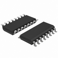
74HC4052D,652 NXP Semiconductors, 74HC4052D,652 Datasheet - Page 8

74HC4052D,652
Manufacturer Part Number
74HC4052D,652
Description
IC MUX/DEMUX DUAL 4X1 16SOIC
Manufacturer
NXP Semiconductors
Series
74HCr
Datasheet
1.74HC4052N652.pdf
(28 pages)
Specifications of 74HC4052D,652
Package / Case
16-SOIC (0.154", 3.90mm Width)
Function
Multiplexer/Demultiplexer
Circuit
2 x 4:1
On-state Resistance
60 Ohm
Voltage Supply Source
Dual Supply
Voltage - Supply, Single/dual (±)
±2 V ~ 10 V
Current - Supply
320µA
Operating Temperature
-40°C ~ 125°C
Mounting Type
Surface Mount
Number Of Channels
2 Channel
On Resistance (max)
150 Ohm (Typ) @ 2 V
On Time (max)
105 ns (Typ) @ 2 V
Off Time (max)
74 ns (Typ) @ 2 V
Supply Voltage (max)
10 V
Supply Voltage (min)
2 V
Maximum Power Dissipation
500 mW
Maximum Operating Temperature
+ 125 C
Minimum Operating Temperature
- 40 C
Mounting Style
SMD/SMT
Number Of Switches
Dual
Lead Free Status / RoHS Status
Lead free / RoHS Compliant
Lead Free Status / RoHS Status
Lead free / RoHS Compliant, Lead free / RoHS Compliant
Other names
568-3962-5
74HC4052D
74HC4052D
933714830652
74HC4052D
74HC4052D
933714830652
NXP Semiconductors
Table 6.
V
V
V
For 74HC4052: V
For 74HCT4052: V
[1]
[2]
74HC_HCT4052
Product data sheet
Symbol
R
I
is
os
Fig 9.
ON(rail)
= V
is the input voltage at a nYn or nZ terminal, whichever is assigned as an input.
is the output voltage at a nYn or nZ terminal, whichever is assigned as an output.
All typical values are measured at T
When supply voltages (V
2 V, it is recommended to use these devices only for transmitting digital signals.
IH
or V
V
Test circuit for measuring R
R
Parameter
ON resistance (rail)
is
R
ON
from select
IL
= 0 V to (V
ON
; for test circuit see
=
resistance per switch for 74HC4052 and 74HCT4052
input
CC
V
-------- -
I
CC
sw
sw
−
−
GND or V
CC
V is
GND = 4.5 V and 5.5 V, V
nYn
Sn
− V
CC
EE
− V
).
GND
V sw
CC
EE
V
Figure
) near 2.0 V the analog switch ON resistance becomes extremely non-linear. When using a supply of
−
amb
V
V
V
CC
EE
EE
nZ
= 25 °C.
ON
9.
Conditions
V
V
= 2.0 V, 4.5 V, 6.0 V and 9.0 V.
001aah826
is
is
All information provided in this document is subject to legal disclaimers.
V
V
V
V
V
V
V
V
= V
= V
CC
CC
CC
CC
CC
CC
CC
CC
I sw
EE
CC
= 2.0 V; V
= 4.5 V; V
= 6.0 V; V
= 4.5 V; V
= 2.0 V; V
= 4.5 V; V
= 6.0 V; V
= 4.5 V; V
CC
Rev. 7 — 12 January 2011
−
V
EE
EE
EE
EE
EE
EE
EE
EE
EE
= 2.0 V, 4.5 V, 6.0 V and 9.0 V.
= 0 V; I
= 0 V; I
= 0 V; I
= −4.5 V; I
= 0 V; I
= 0 V; I
= 0 V; I
= −4.5 V; I
Fig 10. Typical R
Dual 4-channel analog multiplexer/demultiplexer
R
SW
SW
SW
SW
SW
SW
( )
(1) V
(2) V
(3) V
ON
100
74HC4052; 74HCT4052
80
60
40
20
SW
SW
= 100 μA
= 1000 μA
= 1000 μA
= 100 μA
= 1000 μA
= 1000 μA
0
0
…continued
V
= 1000 μA
= 1000 μA
is
CC
CC
CC
= 0 V to (V
= 4.5 V
= 6 V
= 9 V
1.8
ON
CC
as a function of input voltage V
3.6
− V
[2]
[2]
(1)
(2)
(3)
EE
).
Min
-
-
-
-
-
-
-
-
5.4
Typ
-
-
-
-
-
-
-
-
© NXP B.V. 2011. All rights reserved.
7.2
001aai068
V
is
Max
-
210
180
160
-
240
210
180
(V)
9.0
Unit
Ω
Ω
Ω
Ω
Ω
Ω
Ω
Ω
8 of 28
is


