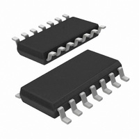
74HC4016D,653 NXP Semiconductors, 74HC4016D,653 Datasheet

74HC4016D,653
Specifications of 74HC4016D,653
74HC4016D-T
933714330653
Related parts for 74HC4016D,653
74HC4016D,653 Summary of contents
Page 1
DATA SHEET For a complete data sheet, please also download: The IC06 74HC/HCT/HCU/HCMOS Logic Family Specifications The IC06 74HC/HCT/HCU/HCMOS Logic Package Information The IC06 74HC/HCT/HCU/HCMOS Logic Package Outlines 74HC/HCT4016 Quad bilateral switches Product specification File under Integrated Circuits, IC06 INTEGRATED ...
Page 2
Philips Semiconductors Quad bilateral switches FEATURES Low “ON” resistance: 160 (typ 4 120 (typ 6 (typ 9 Individual switch controls Typical “break before make” ...
Page 3
Philips Semiconductors Quad bilateral switches PIN DESCRIPTION PIN NO. SYMBOL GND 13 ...
Page 4
Philips Semiconductors Quad bilateral switches Fig.4 Functional diagram. FUNCTION TABLE INPUT CHANNEL E IMPEDANCE n L high H low Notes HIGH voltage level L = LOW voltage level December 1990 APPLICATIONS Signal gating Modulation Demodulation Chopper Fig.5 ...
Page 5
Philips Semiconductors Quad bilateral switches RATINGS Limiting values in accordance with the Absolute Maximum System (IEC 134) Voltages are referenced to GND (ground = 0 V) SYMBOL PARAMETER V DC supply voltage digital input diode current IK ...
Page 6
Philips Semiconductors Quad bilateral switches DC CHARACTERISTICS FOR 74HC/HCT For 74HC 2.0, 4.5, 6.0 and 9 For 74HCT 4 SYMBOL PARAMETER R ON resistance (peak resistance (rail ...
Page 7
Philips Semiconductors Quad bilateral switches Fig.8 Test circuit for measuring ON-state current. Fig.9 Typical R December 1990 as a function of input voltage Product specification 74HC/HCT4016 for ...
Page 8
Philips Semiconductors Quad bilateral switches DC CHARACTERISTICS FOR 74HC Voltages are referenced to GND (ground = 0 V) SYMBOL PARAMETER min. V HIGH level input 1.5 IH voltage 3.15 4.2 6.3 V LOW level input IL voltage I input leakage ...
Page 9
Philips Semiconductors Quad bilateral switches DC CHARACTERISTICS FOR 74HCT Voltages are referenced to GND (ground = 0 V) SYMBOL PARAMETER V HIGH level input 2.0 IH voltage V LOW level input IL voltage I input leakage I current I analog ...
Page 10
Philips Semiconductors Quad bilateral switches AC CHARACTERISTICS FOR 74HCT GND = ns SYMBOL PARAMETER min. typ. max. min. max. min. max propagation delay ...
Page 11
Philips Semiconductors Quad bilateral switches Test conditions 4.5 V; GND = source Fig.10 Typical switch “OFF” signal feed-through as a function of frequency. Test conditions: ...
Page 12
Philips Semiconductors Quad bilateral switches Fig.12 Test circuit for measuring crosstalk between any two switches. (a) channel ON condition; (b) channel OFF condition. The crosstalk is defined as follows (oscilloscope output): Fig.13 Test circuit for measuring crosstalk between control and ...
Page 13
Philips Semiconductors Quad bilateral switches AC WAVEFORMS ( 50 GND HCT 1 GND Fig.16 Waveforms showing the input ...
Page 14
Philips Semiconductors Quad bilateral switches TEST CIRCUIT AND WAVEFORMS Conditions TEST SWITCH t GND V PZH GND PZL CC t GND V PHZ GND PLZ CC others open pulse C = load capacitance including ...


