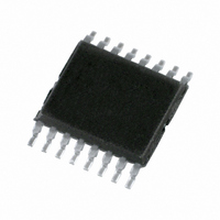
74LV4053PW,118 NXP Semiconductors, 74LV4053PW,118 Datasheet - Page 10

74LV4053PW,118
Manufacturer Part Number
74LV4053PW,118
Description
IC MUX/DEMUX TRIPLE 2X1 16TSSOP
Manufacturer
NXP Semiconductors
Series
74LVr
Type
Analog Multiplexerr
Datasheet
1.74LV4053BQ115.pdf
(26 pages)
Specifications of 74LV4053PW,118
Package / Case
16-TSSOP (0.173", 4.40mm Width)
Function
Multiplexer/Demultiplexer
Circuit
3 x 2:1
On-state Resistance
165 Ohm
Voltage Supply Source
Single Supply
Voltage - Supply, Single/dual (±)
2.7 V ~ 3.6 V
Current - Supply
80µA
Operating Temperature
-40°C ~ 125°C
Mounting Type
Surface Mount
Number Of Channels
3 Channel
On Resistance (max)
180 Ohms
On Time (max)
125 ns
Off Time (max)
95 ns
Supply Voltage (max)
6 V
Supply Voltage (min)
1 V
Maximum Power Dissipation
400 mW
Maximum Operating Temperature
+ 125 C
Minimum Operating Temperature
- 40 C
Mounting Style
SMD/SMT
Number Of Switches
3
Package
16TSSOP
Maximum On Resistance
435@2V Ohm
Maximum Propagation Delay Bus To Bus
25(Typ)@1.2V|9(Typ)@2V|6(Typ)@2.7V|5(Typ)@3.3V|4(Typ)@4.5V|3(Typ)@6V ns
Maximum Low Level Output Current
25 mA
Multiplexer Architecture
2:1
Maximum Turn-off Time
95(Typ)@1.2V ns
Maximum Turn-on Time
125(Typ)@1.2V ns
Power Supply Type
Single
Lead Free Status / RoHS Status
Lead free / RoHS Compliant
Lead Free Status / RoHS Status
Lead free / RoHS Compliant, Lead free / RoHS Compliant
Other names
74LV4053PW-T
74LV4053PW-T
935174970118
74LV4053PW-T
935174970118
NXP Semiconductors
74LV4053_4
Product data sheet
Fig 11. Test circuit for measuring R
Fig 12. Typical R
R
V
i
ON
= 0 V to V
= V
SW
9.3 On resistance waveform and test circuit
ON
/ I
CC
SW
as a function of input voltage
.
V
EE
R
( )
ON
200
150
100
50
0
ON
V
0
IH
or V
GND
IL
Rev. 04 — 10 August 2009
1.2
V
CC
S1 to S3
nZ
I SW
= 2.0 V
E
V
V
CC
CC
2.4
= 3.0 V
nY0
nY1
GND = V
1
2
V SW
Triple single-pole double-throw analog switch
V
EE
3.6
V
CC
switch
V
001aak348
= 4.5 V
I
001aak347
(V)
4.8
V I
74LV4053
© NXP B.V. 2009. All rights reserved.
10 of 26


