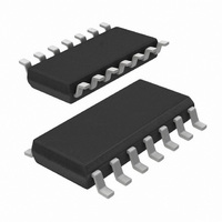
74HC4066D,652 NXP Semiconductors, 74HC4066D,652 Datasheet - Page 6

74HC4066D,652
Manufacturer Part Number
74HC4066D,652
Description
IC SWITCH QUAD 1X2 14SOIC
Manufacturer
NXP Semiconductors
Series
74HCr
Datasheet
1.74HC4066N652.pdf
(27 pages)
Specifications of 74HC4066D,652
Package / Case
14-SOIC (0.154", 3.90mm Width)
Function
Switch
Circuit
4 x 1:2
Voltage Supply Source
Single Supply
Voltage - Supply, Single/dual (±)
2 V ~ 10 V
Current - Supply
40µA
Operating Temperature
-40°C ~ 125°C
Mounting Type
Surface Mount
Switch Configuration
SPST
On Resistance (max)
100 Ohm (Typ) @ 2 V
On Time (max)
36 ns (Typ) @ 2 V
Off Time (max)
44 ns (Typ) @ 2 V
Supply Voltage (max)
10 V
Supply Voltage (min)
2 V
Maximum Power Dissipation
500 mW
Maximum Operating Temperature
+ 125 C
Mounting Style
SMD/SMT
Minimum Operating Temperature
- 40 C
Lead Free Status / RoHS Status
Lead free / RoHS Compliant
Lead Free Status / RoHS Status
Lead free / RoHS Compliant, Lead free / RoHS Compliant
Other names
568-3964-5
74HC4066D
74HC4066D
933714420652
74HC4066D
74HC4066D
933714420652
Philips Semiconductors
RECOMMENDED OPERATING CONDITIONS
LIMITING VALUES
In accordance with the Absolute Maximum Rating System (IEC 60134); voltages are referenced to GND (ground = 0 V).
Notes
1. To avoid drawing V
2. For DIP14 packages: above 70 C derate linearly with 12 mW/K.
2004 Nov 11
V
V
V
T
t
V
I
I
I
I
T
P
P
SYMBOL
SYMBOL
r
IK
SK
S
CC
, t
amb
stg
CC
I
S
CC
tot
S
Quad bilateral switches
f
, I
bidirectional switch must not exceed 0.4 V. If the switch current flows into pin nZ, no V
pin nY. In this case there is no limit for the voltage drop across the switch, but the voltages at pins nY and nZ may
not exceed V
For SO14 packages: above 70 C derate linearly with 8 mW/K.
For SSOP14 and TSSOP16 packages: above 60 C derate linearly with 5.5 mW/K.
For DHVQFN14 packages: above 60 C derate linearly with 4.5 mW/K.
GND
supply voltage
input voltage
switch voltage
ambient temperature
input rise and fall times
supply voltage
input diode current
switch diode current
switch current
V
storage temperature
power dissipation
power dissipation per switch
CC
CC
or GND current
PARAMETER
or GND.
CC
PARAMETER
current out of pin nZ, when switch current flows in pin nY, the voltage drop across the
see DC and AC
characteristics
per device
V
V
V
V
CC
CC
CC
CC
CONDITIONS
= 2.0 V
= 4.5 V
= 6.0 V
= 10.0 V
V
V
T
0.5 V < V
amb
I
S
< 0.5 V or V
< 0.5 V or V
= 40 C to +125 C; note 2
6
2.0
GND
GND
MIN.
40
40
O
CONDITIONS
< V
74HC4066
5.0
+25
6.0
I
CC
TYP.
S
> V
> V
+ 0.5 V; note 1
CC
CC
+ 0.5 V
10.0
V
V
+85
+125
1000
500
400
250
MAX.
+ 0.5 V
CC
CC
74HC4066; 74HCT4066
4.5
GND
GND
MIN.
40
40
CC
74HCT4066
current will flow out of
5.0
+25
6.0
TYP.
MIN.
0.5
65
Product specification
5.5
V
V
+85
+125
500
+11.0
+150
500
100
MAX.
MAX.
20
20
25
50
CC
CC
V
V
V
ns
ns
ns
ns
V
mA
mA
mA
mA
mW
mW
UNIT
UNIT
C
C
C


