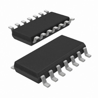
74HC4066D,652 NXP Semiconductors, 74HC4066D,652 Datasheet - Page 9

74HC4066D,652
Manufacturer Part Number
74HC4066D,652
Description
IC SWITCH QUAD 1X2 14SOIC
Manufacturer
NXP Semiconductors
Series
74HCr
Datasheet
1.74HC4066N652.pdf
(27 pages)
Specifications of 74HC4066D,652
Package / Case
14-SOIC (0.154", 3.90mm Width)
Function
Switch
Circuit
4 x 1:2
Voltage Supply Source
Single Supply
Voltage - Supply, Single/dual (±)
2 V ~ 10 V
Current - Supply
40µA
Operating Temperature
-40°C ~ 125°C
Mounting Type
Surface Mount
Switch Configuration
SPST
On Resistance (max)
100 Ohm (Typ) @ 2 V
On Time (max)
36 ns (Typ) @ 2 V
Off Time (max)
44 ns (Typ) @ 2 V
Supply Voltage (max)
10 V
Supply Voltage (min)
2 V
Maximum Power Dissipation
500 mW
Maximum Operating Temperature
+ 125 C
Mounting Style
SMD/SMT
Minimum Operating Temperature
- 40 C
Lead Free Status / RoHS Status
Lead free / RoHS Compliant
Lead Free Status / RoHS Status
Lead free / RoHS Compliant, Lead free / RoHS Compliant
Other names
568-3964-5
74HC4066D
74HC4066D
933714420652
74HC4066D
74HC4066D
933714420652
Philips Semiconductors
Family 74HCT4066
Voltages are referenced to GND (ground = 0 V); V
input; V
Note
1. All typical values are measured at T
2004 Nov 11
T
V
V
I
I
I
I
T
V
V
I
I
I
I
SYMBOL
LI
S(OFF)
S(ON)
CC
LI
S(OFF)
S(ON)
CC
amb
I
amb
I
IH
IL
IH
IL
Quad bilateral switches
CC
CC
= 40 C to +85 C; note 1
= 40 C to +125 C
os
is the output voltage at pins nY or nZ, whichever is assigned as an output.
HIGH-level input
voltage
LOW-level input voltage
input leakage current
analog switch current
OFF-state
analog switch current
ON-state
quiescent supply
current
additional quiescent
supply current per input
HIGH-level input
voltage
LOW-level input voltage
input leakage current
analog switch current
OFF-state
analog switch current
ON-state
quiescent supply
current
additional quiescent
supply current per input
PARAMETER
V
per channel; V
V
V
Fig.8
V
V
V
or GND
V
per channel; V
V
V
Fig.8
V
V
V
or GND
I
S
I
I
os
I
I
S
I
I
os
I
amb
= V
= V
= V
= V
= V
= V
= V
= V
= V
= V
= V
= V
= 25 C.
CC
IH
CC
CC
CC
IH
CC
CC
CC
CC
CC
CC
or V
or V
or GND
or GND; V
or GND
or GND; V
or GND
or GND
2.1 V; other inputs at V
2.1 V; other inputs at V
GND; see Fig.7
GND; see Fig.7
is
IL
IL
is the input voltage at pins nY or nZ, whichever is assigned as an
; V
; V
I
I
TEST CONDITIONS
OTHER
= V
= V
S
S
= V
= V
IH
IH
is
is
9
or V
= GND or V
or V
= GND or V
CC
CC
IL
IL
GND; see
GND; see
;
;
CC
CC
CC
CC
;
;
4.5 to 5.5 2.0
4.5 to 5.5
5.5
5.5
5.5
4.5 to 5.5
4.5 to 5.5
4.5 to 5.5 2.0
4.5 to 5.5
5.5
10.0
10.0
4.5 to 5.5
4.5 to 5.5
74HC4066; 74HCT4066
V
CC
(V)
MIN. TYP. MAX. UNIT
1.6
1.2
100
Product specification
0.8
20.0
450
0.8
40.0
490
1.0
1.0
1.0
1.0
1.0
1.0
V
V
V
V
A
A
A
A
A
A
A
A
A
A


