APT100GT60JR MICROSEMI, APT100GT60JR Datasheet - Page 2
APT100GT60JR
Manufacturer Part Number
APT100GT60JR
Description
Manufacturer
MICROSEMI
Datasheet
1.APT100GT60JR.pdf
(6 pages)
Specifications of APT100GT60JR
Channel Type
N
Configuration
Single
Collector-emitter Voltage
600V
Collector Current (dc) (max)
148A
Gate To Emitter Voltage (max)
±30V
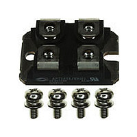
Package Type
SOT-227
Pin Count
4
Mounting
Screw
Operating Temperature (min)
-55C
Operating Temperature (max)
150C
Operating Temperature Classification
Military
Lead Free Status / Rohs Status
Compliant
Available stocks
Company
Part Number
Manufacturer
Quantity
Price
Company:

Part Number:
APT100GT60JR
Manufacturer:
Microsemi Power Products Group
Quantity:
135
Company:
Part Number:
APT100GT60JR
Manufacturer:
ASTEC
Quantity:
560
Company:
Part Number:
APT100GT60JRDQ4
Manufacturer:
Microsemi Power Products Group
Quantity:
135


DYNAMIC CHARACTERISTICS
THERMAL AND MECHANICAL CHARACTERISTICS
1 Repetitive Rating: Pulse width limited by maximum junction temperature.
2 For Combi devices, I
3 See MIL-STD-750 Method 3471.
4 E
5 E
6 E
Symbol
Symbol
V
SSOA
adding to the IGBT turn-on loss. Tested in inductive switching test circuit shown in fi gure 21, but with a Silicon Carbide diode.
loss. (See Figures 21, 22.)
Microsemi Reserves the right to change, without notice, the specifi cations and information contained herein.
V
Isolation
t
t
t
t
R
R
C
E
E
E
E
C
C
Q
Q
d(on)
d(off)
E
d(on)
d(off)
E
W
Q
on1
on2
off
GEP
θ
θ
oes
t
t
on1
on2
t
on1
on2
t
ies
res
off
off
ge
gc
r
r
f
f
g
JC
JC
T
is the clamped inductive turn-off energy measured in accordance with JEDEC standard JESD24-1. (See Figures 21, 23.)
is the clamped inductive turn-on energy of the IGBT only, without the effect of a commutating diode reverse recovery current
is the clamped inductive turn-on energy that includes a commutating diode reverse recovery current in the IGBT turn-on switching
Characteristic
Input Capacitance
Output Capacitance
Reverse Transfer Capacitance
Gate-to-Emitter Plateau Voltage
Total Gate Charge
Gate-Emitter Charge
Gate-Collector ("Miller ") Charge
Switching Safe Operating Area
Turn-on Delay Time
Current Rise Time
Turn-off Delay Time
Current Fall Time
Turn-on Switching Energy
Turn-on Switching Energy (Diode)
Turn-off Switching Energy
Turn-on Delay Time
Current Rise Time
Turn-off Delay Time
Current Fall Time
Turn-on Switching Energy
Turn-on Switching Energy (Diode)
Turn-off Switching Energy
Characteristic
Junction to Case (IGBT)
Junction to Case (DIODE)
Package Weight
RMS Voltage
ces
includes both IGBT and FRED leakages
(50-60hHz Sinusoidal Wavefomr Ffrom Terminals to Mounting Base for 1 Min.)
3
6
4
4
66
4
55
5
T
Inductive Switching (125°C)
15V, L = 100µH,V
Inductive Switching (25°C)
J
= 150°C, R
V
GE
Test Conditions
Capacitance
Gate Charge
T
= 0V, V
V
V
V
T
V
V
V
R
R
f = 1 MHz
I
I
I
J
CC
CC
CE
C
C
J
C
GE
GE
GE
G
G
= +125°C
= +25°C
= 100A
= 100A
= 100A
= 4.3Ω
= 4.3Ω
= 300V
= 400V
= 400V
= 15V
G
= 15V
= 15V
= 4.3Ω, V
CE
CE
= 25V
= 600V
GE
=
2500
300
MIN
MIN
5430
3250
3525
3125
3275
4650
3750
TYP
29.2
508
312
460
210
320
100
350
100
TYP
8.0
40
40
75
40
75
APT100GT60JR
MAX
MAX
N/A
.25
UNIT
UNIT
°C/W
Volts
nC
pF
n
µ
ns
µ
gm
V
A
s
J
J
Related parts for APT100GT60JR
Image
Part Number
Description
Manufacturer
Datasheet
Request
R

Part Number:
Description:
MICROSEMI DIODE
Manufacturer:
MICROSEMI
Datasheet:

Part Number:
Description:
Schottky Rectifier
Manufacturer:
Microsemi Corporation
Datasheet:
Part Number:
Description:
Schottky Rectifier
Manufacturer:
Microsemi Corporation
Datasheet:
Part Number:
Description:
Schottky Rectifier
Manufacturer:
Microsemi Corporation
Datasheet:
Part Number:
Description:
Schottky Rectifier
Manufacturer:
Microsemi Corporation
Datasheet:
Part Number:
Description:
Ultra Fast Rectifier (less than 100ns)
Manufacturer:
Microsemi Corporation
Datasheet:
Part Number:
Description:
Manufacturer:
Microsemi Corporation
Datasheet:
Part Number:
Description:
Ultra Fast Rectifier (less than 100ns)
Manufacturer:
Microsemi Corporation
Datasheet:
Part Number:
Description:
Ultra Fast Rectifier (less than 100ns)
Manufacturer:
Microsemi Corporation
Datasheet:
Part Number:
Description:
Manufacturer:
Microsemi Corporation
Datasheet:
Part Number:
Description:
Manufacturer:
Microsemi Corporation
Datasheet:
Part Number:
Description:
Manufacturer:
Microsemi Corporation
Datasheet:
Part Number:
Description:
Manufacturer:
Microsemi Corporation
Datasheet:
Part Number:
Description:
Manufacturer:
Microsemi Corporation
Datasheet:
Part Number:
Description:
Manufacturer:
Microsemi Corporation
Datasheet: