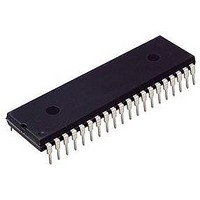
HD3-6402R-9 Intersil, HD3-6402R-9 Datasheet - Page 3

HD3-6402R-9
Manufacturer Part Number
HD3-6402R-9
Description
06F5779
Manufacturer
Intersil
Datasheet
1.HD3-6402R-9Z.pdf
(7 pages)
Specifications of HD3-6402R-9
No. Of Channels
8
Uart Features
Programmable Word Length, Stop Bits And Parity, Automatic Data Formatting And Status Generation
Supply Voltage Range
4.5V To 5.5V
Rohs Compliant
No
Available stocks
Company
Part Number
Manufacturer
Quantity
Price
Company:
Part Number:
HD3-6402R-9
Manufacturer:
N/A
Quantity:
5 704
Company:
Part Number:
HD3-6402R-9
Manufacturer:
N/A
Quantity:
5 704
Part Number:
HD3-6402R-9
Manufacturer:
HAR
Quantity:
20 000
Pin Description
PIN TYPE SYMBOL
10
11
12
13
14
15
16
17
18
19
20
21
22
23
1
2
3
4
5
6
7
8
9
O
O
O
O
O
O
O
O
O
O
O
O
O
I
I
I
I
I
I
I
V
RBR8
RBR7
RBR6
RBR5
RBR4
RBR3
RBR2
RBR1
TBRE
TBRL
GND
RRD
RRC
DRR
SFD
RRI
MR
CC
NC
PE
OE
DR
FE
†
Positive Voltage Supply
No Connection
Ground
A high level on RECEIVER REGISTER DISABLE
forces the receiver holding out-puts RBR1-RBR8
to high impedance state.
The contents of the RECEIVER BUFFER REGIS-
TER appear on these three-state outputs. Word for-
mats less than 8 characters are right justified to
RBR1.
See Pin 5-RBR8
See Pin 5-RBR8
See Pin 5-RBR8
See Pin 5-RBR8
See Pin 5-RBR8
See Pin 5-RBR8
See Pin 5-RBR8
A high level on PARITY ERROR indicates received
parity does not match parity programmed by control
bits. When parity is inhibited this output is low.
A high level on FRAMING ERROR indicates the
first stop bit was invalid.
A high level on OVERRUN ERROR indicates the
data received flag was not cleared before the last
character was transferred to the receiver buffer
register.
A high level on STATUS FLAGS DISABLE forces
the outputs PE, FE, OE, DR, TBRE to a high im-
pedance state.
The Receiver register clock is 16X the receiver
data rate.
A low level on DATA RECEIVED RESET clears
the data received output DR to a low level.
A high level on DATA RECEIVED indicates a
character has been received and transferred to
the receiver buffer register.
Serial data on RECEIVER REGISTER INPUT is
clocked into the receiver register.
A high level on MASTER RESET clears PE, FE,
OE and DR to a low level and sets the transmitter
register empty (TRE) to a high level 18 clock cycles
after MR falling edge. MR does not clear the receiv-
er buffer register. This input must be pulsed at least
once after power up. The HD-6402 must be master
reset after power up. The reset pulse should meet
V
edge of MR before beginning operation.
A high level on TRANSMITTER BUFFER REGIS-
TER EMPTY indicates the transmitter buffer register
has transferred its data to the transmitter register
and is ready for new data.
A low level on TRANSMITTER BUFFER REGIS-
TER LOAD transfers data from inputs TBR1-
TBR8 into the transmitter buffer register. A low to
high transition on TBRL initiates data transfer to
the transmitter register. If busy, transfer is auto-
matically delayed so that the two characters are
transmitted end to end.
IH
and t
MR
. Wait 18 clock cycles after the falling
3
DESCRIPTION
HD-6402
HD-6402
PIN TYPE SYMBOL
† A 0.1µF decoupling capacitor from the V
24
25
26
27
28
29
30
31
32
33
34
35
36
37
38
39
40
recommended.
O
O
I
I
I
I
I
I
I
I
I
I
I
I
I
I
I
TRB1
TBR2
TBR3
TBR4
TBR5
TBR6
TBR7
TBR8
CLS2
CLS1
TRO
TRC
TRE
CRL
SBS
EPE
PI
A high level on TRANSMITTER REGISTER EMP-
TY indicates completed transmission of a charac-
ter including stop bits.
Character data, start data and stop bits appear se-
rially at the TRANSMITTER REGISTER OUTPUT.
Character data is loaded into the TRANSMITTER
BUFFER REGISTER via inputs TBR1-TBR8. For
character formats less than 8 bits the TBR8, 7 and
6 inputs are ignored corresponding to their pro-
grammed word length.
See Pin 26-TBR1.
See Pin 26-TBR1.
See Pin 26-TBR1.
See Pin 26-TBR1.
See Pin 26-TBR1.
See Pin 26-TBR1.
See Pin 26-TBR1.
A high level on CONTROL REGISTER LOAD
loads the control register with the control word. The
control word is latched on the falling edge of CRL.
CRL may be tied high.
A high level on PARITY INHIBIT inhibits parity gen-
eration, parity checking and forces PE output low.
A high level on STOP BIT SELECT selects 1.5
stop bits for 5 character format and 2 stop bits for
other lengths.
These inputs program the CHARACTER
LENGTH SELECTED (CLS1 low CLS2 low 5 bits)
(CLS1 high CLS2 low 6 bits) (CLS1 low CLS2
high 7 bits) (CLS1 high CLS2 high 8 bits.)
See Pin 37-CLS2.
When PI is low, a high level on EVEN PARITY
ENABLE generates and checks even parity. A low
level selects odd parity.
The TRANSMITTER REGISTER CLOCK is 16X
the transmit data rate.
DESCRIPTION
CC
pin to the GND is


