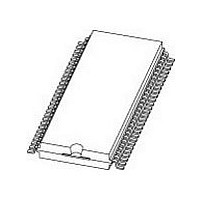
PCF8576CT NXP Semiconductors, PCF8576CT Datasheet - Page 24

PCF8576CT
Manufacturer Part Number
PCF8576CT
Description
Manufacturer
NXP Semiconductors
Datasheet
1.PCF8576CT.pdf
(56 pages)
Specifications of PCF8576CT
Operating Supply Voltage (typ)
2.5/3.3/5V
Number Of Digits
20
Number Of Segments
160
Package Type
VSO
Pin Count
56
Mounting
Surface Mount
Power Dissipation
400mW
Frequency (max)
315KHz
Operating Supply Voltage (min)
2V
Operating Supply Voltage (max)
6V
Lead Free Status / Rohs Status
Compliant
Available stocks
Company
Part Number
Manufacturer
Quantity
Price
Part Number:
PCF8576CT
Manufacturer:
PHILIPS/飞利浦
Quantity:
20 000
Part Number:
PCF8576CT/1
Manufacturer:
NXP/恩智浦
Quantity:
20 000
Part Number:
PCF8576CT/1,518
Manufacturer:
NXP/恩智浦
Quantity:
20 000
Company:
Part Number:
PCF8576CT/1112
Manufacturer:
NXP Semiconductors
Quantity:
135
Company:
Part Number:
PCF8576CT/1118
Manufacturer:
NXPSemicondu
Quantity:
2 802
Company:
Part Number:
PCF8576CT/1Ј¬112
Manufacturer:
NXP
Quantity:
880
Company:
Part Number:
PCF8576CT/1Ј¬118
Manufacturer:
NXP
Quantity:
21 000
Part Number:
PCF8576CT/F1
Manufacturer:
PHILIPS/飞利浦
Quantity:
20 000
Part Number:
PCF8576CTT
Manufacturer:
NXP/恩智浦
Quantity:
20 000
NXP Semiconductors
PCF8576C_9
Product data sheet
8.1.3 Acknowledge
The number of data bytes transferred between the START and STOP conditions from
transmitter to receiver is unlimited. Each byte of eight bits is followed by an acknowledge
bit. The acknowledge bit is a HIGH level signal put on the bus by the transmitter during
which time the master generates an extra acknowledge related clock pulse.
Acknowledgement on the I
Fig 16. System configuration
Fig 17. Acknowledgement on the I
•
•
•
•
A slave receiver which is addressed must generate an acknowledge after the
reception of each byte.
A master receiver must generate an acknowledge after the reception of each byte that
has been clocked out of the slave transmitter.
The device that acknowledges must pull-down the SDA line during the acknowledge
clock pulse, so that the SDA line is stable LOW during the HIGH period of the
acknowledge related clock pulse (set-up and hold times must be taken into
consideration).
A master receiver must signal an end-of-data to the transmitter by not generating an
acknowledge on the last byte that has been clocked out of the slave. In this event, the
master receiver must leave the data line HIGH during the 9th pulse to not
acknowledge. The master will now generate a STOP condition.
SCL
SDA
by transmitter
data output
by receiver
data output
TRANSMITTER/
SCL from
RECEIVER
master
MASTER
condition
START
S
Rev. 09 — 9 July 2009
2
RECEIVER
C-bus is illustrated in
SLAVE
1
2
C-bus
TRANSMITTER/
RECEIVER
Universal LCD driver for low multiplex rates
SLAVE
2
Figure
TRANSMITTER
17.
MASTER
not acknowledge
acknowledge
8
PCF8576C
acknowledgement
clock pulse for
TRANSMITTER/
© NXP B.V. 2009. All rights reserved.
RECEIVER
MASTER
9
mbc602
mga807
24 of 56


