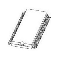
PCF8579T NXP Semiconductors, PCF8579T Datasheet - Page 15

PCF8579T
Manufacturer Part Number
PCF8579T
Description
Manufacturer
NXP Semiconductors
Datasheet
1.PCF8579T.pdf
(41 pages)
Specifications of PCF8579T
Operating Supply Voltage (typ)
3.3/5V
Operating Temperature (min)
-40C
Operating Temperature (max)
85C
Operating Temperature Classification
Industrial
Package Type
VSO
Pin Count
56
Mounting
Surface Mount
Power Dissipation
400mW
Operating Supply Voltage (min)
2.5V
Operating Supply Voltage (max)
6V
Lead Free Status / Rohs Status
Not Compliant
Available stocks
Company
Part Number
Manufacturer
Quantity
Price
Part Number:
PCF8579T
Manufacturer:
PHILIPS/飞利浦
Quantity:
20 000
Company:
Part Number:
PCF8579T/1
Manufacturer:
NXP
Quantity:
550
Company:
Part Number:
PCF8579T/1118
Manufacturer:
NXP
Quantity:
655
NXP Semiconductors
PCF8579_5
Product data sheet
8.6.5 I
8.6.6 Input filters
8.6.7 I
The I
data bytes. It performs the conversion of the data input (serial-to-parallel) and the data
output (parallel-to-serial). The PCF8579 acts as an I
Device selection depends on the I
the commands transmitted.
To enhance noise immunity in electrically adverse environments, RC low-pass filters are
provided on the SDA and SCL lines.
Two 7-bit slave addresses (0111100 and 0111101) are reserved for both the PCF8578
and PCF8579. The least significant bit of the slave address is set by connecting input SA0
to either logic 0 (V
be distinguished on the same I
In most applications the PCF8578 will have the same slave address as the PCF8579.
The I
condition (S) from the I
read/write bit. All devices with this slave address acknowledge in parallel. All other devices
ignore the bus transfer.
In WRITE mode (indicated by setting the read/write bit LOW) one or more commands
follow the slave address acknowledgement. The commands are also acknowledged by all
addressed devices on the bus. The last command must clear the continuation bit C.
After the last command a series of data bytes may follow. The acknowledgement after
each byte is made only by the (A0, A1, A2 and A3) addressed PCF8579 or PCF8578 with
its implicit subaddress 0. After the last data byte has been acknowledged, the I
master issues a STOP condition (P).
In READ mode, indicated by setting the read/write bit HIGH, data bytes may be read from
the RAM following the slave address acknowledgement. After this acknowledgement the
master transmitter becomes a master receiver and the PCF8579 becomes a slave
transmitter. The master receiver must acknowledge the reception of each byte in turn. The
master receiver must signal an end of data to the slave transmitter, by not generating an
acknowledge on the last byte clocked out of the slave. The slave transmitter then leaves
the data line HIGH, enabling the master to generate a STOP condition (P).
Display bytes are written into, or read from the RAM at the address specified by the data
pointer and subaddress counter. Both the data pointer and subaddress counter are
automatically incremented, enabling a stream of data to be transferred either to, or from
the intended devices.
2
2
1. One PCF8578 to operate with up to 32 PCF8579s on the same I
2. The use of two types of LCD multiplex schemes on the same I
C-bus controller
C-bus protocol
applications (see
2
2
C-bus controller detects the I
C-bus protocol is shown in
SS
) or logic 1 (V
Table
2
Rev. 05 — 11 May 2009
C-bus master, which is followed by the desired slave address and
16).
2
C-bus which allows:
Figure
2
DD
2
C-bus slave address, the hardware subaddress and
C-bus protocol, slave address, commands and display
LCD column driver for dot matrix graphic displays
). Therefore, two types of PCF8578 or PCF8579 can
13. All communications are initiated with a START
2
C-bus slave transmitter/receiver.
2
C-bus.
2
C-bus for very large
PCF8579
© NXP B.V. 2009. All rights reserved.
2
C-bus
15 of 41


