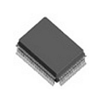
IDT821068PX IDT, Integrated Device Technology Inc, IDT821068PX Datasheet - Page 30

IDT821068PX
Manufacturer Part Number
IDT821068PX
Description
Manufacturer
IDT, Integrated Device Technology Inc
Type
General Purposer
Datasheet
1.IDT821068PX.pdf
(45 pages)
Specifications of IDT821068PX
Number Of Adc's
8
Number Of Dac's
8
Interface Type
Serial
Power Supply Type
Analog/Digital
Operating Supply Voltage (min)
4.75V
Operating Supply Voltage (typ)
5V
Operating Supply Voltage (max)
5.25V
Pin Count
128
Operating Temperature (min)
-40C
Operating Temperature (max)
85C
Screening Level
Industrial
Package Type
PQFP
Mounting
Surface Mount
Lead Free Status / Rohs Status
Not Compliant
Available stocks
Company
Part Number
Manufacturer
Quantity
Price
Company:
Part Number:
IDT821068PX
Manufacturer:
IDT
Quantity:
5 510
Company:
Part Number:
IDT821068PX
Manufacturer:
SANYO
Quantity:
5 510
Company:
Part Number:
IDT821068PX
Manufacturer:
IDT
Quantity:
359
Part Number:
IDT821068PX
Manufacturer:
IDT
Quantity:
20 000
Company:
Part Number:
IDT821068PX8
Manufacturer:
IDT
Quantity:
5 510
Company:
Part Number:
IDT821068PX8
Manufacturer:
DALLAS
Quantity:
5 510
Local Commands:
1. Coefficient Select (00H/80H), Read/Write
Filter, Echo Cancellation Filter, High-Pass Filter, Gain for Impedance Scaling, Gain in Transmit/Receive Path and Frequency Response Correc-
tion in Transmit/Receive Path. See Figure 9 for detail. It should be noted that Impedance Matching Filter and Gain for Impedance Scaling are
working together to adjust impedance. That is to say, CS[0] and CS[2] should be set to the same value to ensure the correct operation.
2. Loop Status Control, PCM Receive Path Cutoff and SLIC Input Interrupt Enable (01H/81H), Read/Write
IDT821068 OCTAL PROGRAMMABLE PCM CODEC
Coefficient Select bits (CS[7:0]) are used to control digital filters and function blocks on corresponding channel such as Impedance Matching
The mapping method of RAM can be found in Coefficient Memory Address Mapping (Page 42).
Loop Status Control Bits (LPC[2:0]) determine the loopback status on corresponding channel.
PCM Receive Path Cutoff bit (PCF) is used to cut off the PCM receive path, see Figure 9.
SLIC Input Interrupt Enable bits (IE[3:0]) enable or disable the interrupt signal on each channel.
CS[0] = 0: Impedance Matching Filter is disabled (default);
CS[0] = 1: Impedance Matching Filter coefficient is set by IMF RAM;
CS[1] = 0: Echo Cancellation Filter is disabled (default);
CS[1] = 1: Echo Cancellation Filter coefficient is set by ECF RAM;
CS[2] = 0: Gain for Impedance Scaling is disabled (default);
CS[2] = 1: Gain for Impedance Scaling coefficient is set by GIS RAM;
CS[3] = 0: High-Pass Filter is bypassed/disabled;
CS[3] = 1: High-Pass Filter is enabled (default);
CS[4] = 0: Frequency Response Correction in Transmit Path is bypassed (default);
CS[4] = 1: Frequency Response Correction in Transmit Path coefficient is set by FRX RAM;
CS[5] = 0: Gain in Transmit Path is 0 dB (default);
CS[5] = 1: Gain in Transmit Path coefficient is set by GTX RAM;
CS[6] = 0: Frequency Response Correction in Receive Path is bypassed (default);
CS[6] = 1: Frequency Response Correction in Receive Path coefficient is set by FRR RAM;
CS[7] = 0: Gain in Receive Path is 0 dB (default);
CS[7] = 1: Gain in Receive Path coefficient is set by GRX RAM.
LPC[0] = 0: Digital Loopback via Onebit is disabled on the corresponding channel (default);
LPC[0] = 1: Digital loopback via Onebit is enabled on the corresponding channel;
LPC[1] = 0: Analog Loopback via Onebit is disabled on the corresponding channel (default);
LPC[1] = 1: Analog Loopback via Onebit is enabled on the corresponding channel;
LPC[2] = 0: Digital Loopback via Time slots is disabled on the corresponding channel (default);
LPC[2] = 1: Digital Loopback via Time slots is enabled on the corresponding channel. In this loopback mode, the digital data received
PCF = 0: PCM Receive Path in normal operation;
PCF = 1: PCM Receive Path is cut off.
IE[0] = 0: Interrupt disable. Interrupt signal on SB2 (when it is selected as an input) will be ignored (default);
IE[0] = 1: Interrupt enable. Interrupt signal on SB2 (when it is selected as an input) will be recognized;
IE[1] = 0: Interrupt disable. Interrupt signal on SB1 (when it is selected as an input) will be ignored (default);
IE[1] = 1: Interrupt enable. Interrupt signal on SB1 (when it is selected as an input) will be recognized;
IE[2] = 0: Interrupt disable. Interrupt signal on SI2 will be ignored (default);
IE[2] = 1: Interrupt enable. Interrupt signal on SI2 will be recognized;
IE[3] = 0: Interrupt disable. Interrupt signal on SI1 will be ignored (default);
IE[3] = 1: Interrupt enable. Interrupt signal on SI1 will be recognized;
Command
Command
I/O data
I/O data
from DR will be switched by the time slot setting, and then will be transmitted out from DX pin.
CS[7]
IE[3]
R /W
R /W
b7
b7
CS[6]
IE[2]
b6
b6
0
0
CS[5]
IE[1]
b5
b5
0
0
30
CS[4]
IE[0]
b4
b4
0
0
CS[3]
PCF
b3
b3
0
0
LPC[2]
CS[2]
b2
b2
0
0
INDUSTRIAL TEMPERATURE RANGE
LPC[1]
CS[1]
b1
b1
0
0
LPC[0]
CS[0]
b0
b0
0
1


