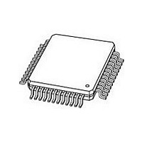
"CX24109-11Z,518" NXP Semiconductors, "CX24109-11Z,518" Datasheet - Page 21

"CX24109-11Z,518"
Manufacturer Part Number
"CX24109-11Z,518"
Description
Manufacturer
NXP Semiconductors
Datasheet
1.CX24109-11Z518.pdf
(40 pages)
Specifications of "CX24109-11Z,518"
Lead Free Status / Rohs Status
Compliant
- Current page: 21 of 40
- Download datasheet (250Kb)
NXP Semiconductors
Table 7.
1.7.1
CX24109_N_1
Product data sheet
Bit 15
Bit 18
0
0
1
1
0
0
1
1
PLL Programming
Gain Equations
Bit 16
0
1
The RF block voltage gain (G
G
VGA1 voltage gain G
VGA2 voltage gain G
The total baseband voltage gain G
G
G
G
where the maximum value of G
RF
VGA1
VGA2
Baseband
Bit 14
Bit 17
=
0
1
0
1
0
1
0
1
=
=
V
AGC
V
=
=
VGA2 Offset
AGC
G
G
×
VGA1
VGA1
VCA Slope VCA Offset in dB
×
26
(
(
+ +
+
+
3
G
Rev. 01 — 13 November 2008
VGA1
VGA2
Charge Pump Current
Charge Pump Polarity
VGA1 Offset in dB
Filter
Reference Dividers
(
in dB
G
) is equal to
) is equal to
VGA2
–
+
G
)
(
RF
VGA2
RF
Baseband
is 23 dB, regardless of voltage
) is equal to the VCA gain + the mixer gain.
(
) is equal to
(
)
)
+
Current (mA)
23
Function
Function
Reserved
Reserved
Negative
Positive
÷10
—
1
2
3
4
Chapter 1: Functional Description
CX24109
© NXP B.V. 2008. All rights reserved.
21
Related parts for "CX24109-11Z,518"
Image
Part Number
Description
Manufacturer
Datasheet
Request
R
Part Number:
Description:
Manufacturer:
NXP Semiconductors
Datasheet:
Part Number:
Description:
Manufacturer:
NXP Semiconductors
Datasheet:

Part Number:
Description:
IC SATELLITE TUNER DGTL 48-ETQFP
Manufacturer:
NXP Semiconductors
Datasheet:

Part Number:
Description:
IC SATELLITE TUNER DGTL 48-ETQFP
Manufacturer:
NXP Semiconductors
Datasheet:
Part Number:
Description:
NXP Semiconductors designed the LPC2420/2460 microcontroller around a 16-bit/32-bitARM7TDMI-S CPU core with real-time debug interfaces that include both JTAG andembedded trace
Manufacturer:
NXP Semiconductors
Datasheet:

Part Number:
Description:
NXP Semiconductors designed the LPC2458 microcontroller around a 16-bit/32-bitARM7TDMI-S CPU core with real-time debug interfaces that include both JTAG andembedded trace
Manufacturer:
NXP Semiconductors
Datasheet:
Part Number:
Description:
NXP Semiconductors designed the LPC2468 microcontroller around a 16-bit/32-bitARM7TDMI-S CPU core with real-time debug interfaces that include both JTAG andembedded trace
Manufacturer:
NXP Semiconductors
Datasheet:
Part Number:
Description:
NXP Semiconductors designed the LPC2470 microcontroller, powered by theARM7TDMI-S core, to be a highly integrated microcontroller for a wide range ofapplications that require advanced communications and high quality graphic displays
Manufacturer:
NXP Semiconductors
Datasheet:
Part Number:
Description:
NXP Semiconductors designed the LPC2478 microcontroller, powered by theARM7TDMI-S core, to be a highly integrated microcontroller for a wide range ofapplications that require advanced communications and high quality graphic displays
Manufacturer:
NXP Semiconductors
Datasheet:
Part Number:
Description:
The Philips Semiconductors XA (eXtended Architecture) family of 16-bit single-chip microcontrollers is powerful enough to easily handle the requirements of high performance embedded applications, yet inexpensive enough to compete in the market for hi
Manufacturer:
NXP Semiconductors
Datasheet:
Part Number:
Description:
The XA-S3 device is a member of Philips Semiconductors? XA(eXtended Architecture) family of high performance 16-bitsingle-chip microcontrollers
Manufacturer:
NXP Semiconductors
Datasheet:

Part Number:
Description:
The NXP BlueStreak LH75401/LH75411 family consists of two low-cost 16/32-bit System-on-Chip (SoC) devices
Manufacturer:
NXP Semiconductors
Datasheet:

Part Number:
Description:
The NXP LPC3130/3131 combine an 180 MHz ARM926EJ-S CPU core, high-speed USB2
Manufacturer:
NXP Semiconductors
Datasheet:


