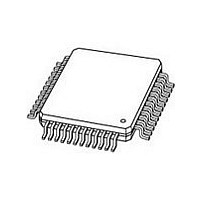
"CX24109-11Z,518" NXP Semiconductors, "CX24109-11Z,518" Datasheet - Page 33

"CX24109-11Z,518"
Manufacturer Part Number
"CX24109-11Z,518"
Description
Manufacturer
NXP Semiconductors
Datasheet
1.CX24109-11Z518.pdf
(40 pages)
Specifications of "CX24109-11Z,518"
Lead Free Status / Rohs Status
Compliant
NXP Semiconductors
Figure 15.
Table 15.
CX24109_N_1
Product data sheet
Tuning Frequency
Input Power, Single Tone
Aggregate Input Power
Input Impedance, Balanced
Input VSWR
Iout and Qout Output Voltage
Maximum Conversion (Voltage) Gain
Minimum Conversion (Voltage) Gain
Noise Figure (NF)
Enable
Clock
Data
(1)
RF Electrical Characteristics (Sheet 1 of 3)
Serial Programming Example
(1) (3)
Parameter
(1)(2)
(1)
t
(1)
HD
t
su
Rev. 01 — 13 November 2008
Depends on bandwidth of incoming signal
and C/I
Z
R
Pin = –43 dBm,
1–5 MSps gain coefficients
Pin = –81 dBm,
1–5 MSps gain coefficients
Pin = –34.5 dBm,
5–15 MSps gain coefficients
Pin = –72 dBm,
5–15 MSps gain coefficients
Pin = –30 dBm,
15–45 MSps gain coefficients
Pin = –70 dBm,
15–45 MSps gain coefficients
V
V
SOURCE
Load
AGC
AGC
=2.4 V, 1 MSps gain coefficients
=1.45 V, 45 MSps gain coefficients
= 1 kΩ
. . .
. . .
= 75 Ω
Conditions
—
—
—
Chapter 3: Parametric Data and Specifications
(4)
(5)
(6)
(7)
(8)
(9)
(1)
(1)
Min
950
–81
—
—
—
—
76
—
—
—
—
—
—
8
t
10.5
10.5
10.5
Typ
ce
0.5
75
10
86
35
35
—
—
—
18
36
t
CX24109
ew
2150
Max
© NXP B.V. 2008. All rights reserved.
–23
–7
91
23
42
14
42
14
45
14
—
—
—
102031_016
Units
MHz
dBm
dBm
V
dB
dB
dB
dB
dB
dB
dB
dB
dB
Ω
P-P
33


