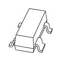
BF909 NXP Semiconductors, BF909 Datasheet - Page 6

BF909
Manufacturer Part Number
BF909
Description
Enhancement type Field-Effect Transistor in a plastic SOT143 package
Manufacturer
NXP Semiconductors
Datasheet
1.BF909.pdf
(12 pages)
Specifications of BF909
Application
VHF/UHF
Channel Type
N
Channel Mode
Enhancement
Continuous Drain Current
0.04A
Drain Source Voltage (max)
7V
Noise Figure (max)
2.8dB
Frequency (max)
1GHz
Package Type
SOT-143B
Pin Count
3 +Tab
Input Capacitance (typ)@vds
3.6@5V@Gate 1/2.3@5V@Gate 2pF
Output Capacitance (typ)@vds
2.3@5VpF
Reverse Capacitance (typ)
0.035@5VpF
Operating Temp Range
-65C to 150C
Mounting
Surface Mount
Number Of Elements
2
Power Dissipation (max)
200@Ta=50CmW
Screening Level
Military
Lead Free Status / Rohs Status
Compliant
Available stocks
Company
Part Number
Manufacturer
Quantity
Price
Part Number:
BF909
Manufacturer:
PHILIPS/NXP
Quantity:
20 000
Part Number:
BF909AR
Manufacturer:
NXP/恩智浦
Quantity:
20 000
Company:
Part Number:
BF909R
Manufacturer:
NXP
Quantity:
57 000
Part Number:
BF909R
Manufacturer:
NXP/恩智浦
Quantity:
20 000
Company:
Part Number:
BF909R(M2P)
Manufacturer:
TI
Quantity:
358
Part Number:
BF909R-TL
Manufacturer:
PHILIPS/飞利浦
Quantity:
20 000
Company:
Part Number:
BF909WR
Manufacturer:
NXP
Quantity:
60 000
Part Number:
BF909WR
Manufacturer:
PHILIPS/飞利浦
Quantity:
20 000
NXP Semiconductors
handbook, halfpage
handbook, halfpage
N-channel dual gate MOS-FETs
V
T
V
R
j
DS
DS
G1
(mS)
(mA)
= 25 C.
y fs
I D
Fig.8
= 5 V.
= 5 V; V
= 120 k (connected to V
Fig.10 Drain current as a function of gate 1
16
12
60
40
20
0
8
4
0
0
0
G2-S
Forward transfer admittance as a
function of drain current; typical values.
supply voltage (= V
see Fig.18.
= 4 V.
10
2
GG
); T
j
= 25 C.
GG
20
); typical values;
4
V
G2 S
V
I
D
GG
(mA)
3.5 V
3 V
2.5 V
MLB942
(V)
2 V
= 4 V
MLB940
Rev. 02 - 19 November 2007
30
6
handbook, halfpage
handbook, halfpage
V
T
V
R
Fig.9
j
DS
G2-S
(mA)
G1
= 25 C.
(mA)
I D
I D
= 5 V; V
connected to V
Fig.11 Drain current as a function of gate 1
25
20
15
10
30
20
10
= 4 V.
5
0
0
0
0
Drain current as a function of gate 1 current;
typical values.
G2-S
(= V
typical values; see Fig.18.
= 4 V.
GG
GG
2
; T
R
j
) and drain supply voltage;
G1
20
= 25 C.
= 47 k
4
BF909; BF909R
68 k
V
GG
40
Product specification
= V
6
I
G1
DS
( A)
100 k
120 k
150 k
180 k
220 k
(V)
82 k
MLB943
MLB941
6 of 12
60
8


