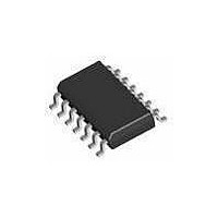
HEF4001BTD NXP Semiconductors, HEF4001BTD Datasheet - Page 6

HEF4001BTD
Manufacturer Part Number
HEF4001BTD
Description
Gates (AND / NAND / OR / NOR) QUAD 2-IN NOR GATE
Manufacturer
NXP Semiconductors
Datasheet
1.HEF4001BP652.pdf
(11 pages)
Specifications of HEF4001BTD
Product
NOR
Logic Family
HE4000B
Number Of Gates
Quad
Number Of Lines (input / Output)
8 / 4
High Level Output Current
- 3.6 mA
Low Level Output Current
3.6 mA
Propagation Delay Time
25 ns
Supply Voltage (max)
15 V
Supply Voltage (min)
3 V
Maximum Operating Temperature
+ 85 C
Mounting Style
SMD/SMT
Package / Case
SOT-108
Minimum Operating Temperature
- 40 C
Lead Free Status / Rohs Status
Details
Other names
HEF4001BT,652
NXP Semiconductors
12. Waveforms
Table 9.
Table 10.
HEF4001B_7
Product data sheet
Supply voltage
V
5 V to 15 V
Supply voltage
V
5 V to 15 V
Fig 4.
Fig 5.
DD
DD
Measurement points are given in
Logic levels: V
Propagation delay, output transition time
Test data is given in
Definitions for test circuit:
DUT = Device Under Test.
C
R
Test circuit for measuring switching times
L
T
Measurement points
Test data
= load capacitance including jig and probe capacitance.
= termination resistance should be equal to the output impedance Z
OL
and V
Table
Input
V
V
OH
I
SS
are typical output voltage levels that occur with the output load.
10.
or V
output
DD
input
Table
Input
V
0.5V
G
M
V
V
0 V
OH
OL
V
9.
DD
I
V
10 %
Rev. 07 — 27 October 2009
I
90 %
R T
V
90 %
M
t
DUT
V
r
V
DD
10 %
M
t
PHL
t
t
THL
r
, t
20 ns
f
V
O
C L
o
of the pulse generator.
001aag182
t
f
001aag197
t
PLH
t
TLH
Output
V
0.5V
M
DD
Load
C
50 pF
L
Quad 2-input NOR gate
HEF4001B
© NXP B.V. 2009. All rights reserved.
6 of 11


