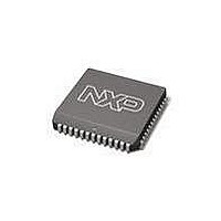
SC28C94A1A NXP Semiconductors, SC28C94A1A Datasheet - Page 26

SC28C94A1A
Manufacturer Part Number
SC28C94A1A
Description
UART Interface IC UART QUAD W/FIFO
Manufacturer
NXP Semiconductors
Type
Quad UARTr
Datasheet
1.SC28C94A1A512.pdf
(39 pages)
Specifications of SC28C94A1A
Number Of Channels
4
Data Rate
1 Mbps
Supply Voltage (max)
5.5 V
Supply Voltage (min)
4.5 V
Supply Current
35 mA
Maximum Operating Temperature
+ 85 C
Minimum Operating Temperature
- 40 C
Package / Case
PLCC-52
Description/function
Quad UART
Mounting Style
SMD/SMT
Operating Supply Voltage
5 V
Lead Free Status / Rohs Status
Details
Other names
SC28C94A1A,512
Available stocks
Company
Part Number
Manufacturer
Quantity
Price
Company:
Part Number:
SC28C94A1A,512
Manufacturer:
NXP Semiconductors
Quantity:
10 000
Company:
Part Number:
SC28C94A1A,518
Manufacturer:
Maxim
Quantity:
21
Company:
Part Number:
SC28C94A1A,518
Manufacturer:
NXP Semiconductors
Quantity:
10 000
1. Parameters are valid over specified temperature range. See ordering information table for applicable temperature range and operating
Philips Semiconductors
AC ELECTRICAL CHARACTERISTICS
V
NOTES:
2. Timing is illustrated and referenced to the WRN and RDN inputs. The device may also be operated with CEN as a ‘strobing’ input. CEN and
3. The RDN signal must be negated for this time to guarantee that internal registers update before the next read.
2006 Aug 09
CC
Quad universal asynchronous receiver/transmitter (QUART)
NO
NO.
supply range.
RDN (also CEN and WRN) are ANDed internally. As a consequence the signal asserted last initiates the cycle; the signal negated first
terminates the cycle. Address is latched at leading edge of a read or write cycle.
10
1
2
3
4
5
6
7
8
9
= 5 V
A[5:0]
D[7:0]
WRN
CEN
RDN
FIGURE
FIGURE
10 %, T
4
4
4
4
4
4
4
4
4
4
A
= –40 C to 85 C, unless otherwise specified.
A[5:0] Setup time to RDN WRN Low
A[5:0] Hold time from RDN WRN Low
CEN Setup time to RDN WRN Low
CEN Hold time from RDN WRN High
RDN WRN Pulse Width Low
D[7:0] Data Valid after CEN and RDN Low
D[7:0] Data Bus floating after RDN or CEN High
D[7:0] Data Bus Setup time before WRN or CEN High
D[7:0] Hold time after WRN or CEN High
Time between Reads and/or Writes
1
3
2
Figure 4. A Read Cycle Followed by a Write Cycle without DACKN
6
5
CHARACTERISTIC
CHARACTERISTIC
1
READ CYCLE
2
3
2
4
7
26
10
1
2
WRITE CYCLE
Min
45
65
20
5
0
0
0
5
0
8
LIMITS
Typ
9
Max
SC28C94
65
10
Product data sheet
SD00164
UNIT
UNIT
ns
ns
ns
ns
ns
ns
ns
ns
ns
ns


