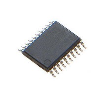
ATTINY861A-XU Atmel, ATTINY861A-XU Datasheet - Page 123

ATTINY861A-XU
Manufacturer Part Number
ATTINY861A-XU
Description
Microcontrollers (MCU) 8K Flash;125B EEPROM 128B SRAM;16 IO Pins
Manufacturer
Atmel
Datasheet
1.ATTINY861A-XU.pdf
(292 pages)
Specifications of ATTINY861A-XU
Core
RISC
Data Bus Width
8 bit
Program Memory Type
Flash
Program Memory Size
8 KB
Data Ram Size
512 B
Interface Type
SPI
Maximum Clock Frequency
20 MHz
Number Of Programmable I/os
16
Operating Supply Voltage
1.8 V to 5.5 V
Maximum Operating Temperature
+ 85 C
Mounting Style
SMD/SMT
Package / Case
TSSOP-20
Minimum Operating Temperature
- 40 C
Lead Free Status / Rohs Status
Details
Available stocks
Company
Part Number
Manufacturer
Quantity
Price
Company:
Part Number:
ATTINY861A-XUR
Manufacturer:
IDT
Quantity:
1 300
- Current page: 123 of 292
- Download datasheet (9Mb)
13. USI – Universal Serial Interface
13.1
13.2
8197B–AVR–01/10
Features
Overview
•
•
•
•
•
•
The Universal Serial Interface, or USI, provides the basic hardware resources needed for serial
communication. Combined with a minimum of control software, the USI allows significantly
higher transfer rates and uses less code space than solutions based on software only. Interrupts
are included to minimize the processor load.
A simplified block diagram of the USI is shown in
refer to
tions are listed in the
Figure 13-1. Universal Serial Interface, Block Diagram
The 8-bit USI Data Register (USIDR) is directly accessible via the data bus and contains the
incoming and outgoing data. The register has no buffering so the data must be read as quickly
as possible to ensure that no data is lost. The data register is a serial shift register where the
most significant bit is connected to one of two output pins depending of the wire mode configura-
tion. A transparent latch between the output of the data register and the output pin delays the
change of data output to the opposite clock edge of the data input sampling. The serial input is
always sampled from the Data Input (DI) pin, regardless of the configuration.
Two-wire Synchronous Data Transfer (Master or Slave)
Three-wire Synchronous Data Transfer (Master or Slave)
Data Received Interrupt
Wakeup from Idle Mode
In Two-wire Mode: Wake-up from All Sleep Modes, Including Power-down Mode
Two-wire Start Condition Detector with Interrupt Capability
“Pinout ATtiny261A/461A/861A” on page
USIDR
USICR
USIDB
USISR
2
“Register Descriptions” on page
4-bit Counter
3
2
1
0
3
2
1
0
D Q
LE
[1]
TIM0 COMP
Figure 13-1
0
1
2. Device-specific I/O Register and bit loca-
130.
Two-wire Clock
Control Unit
For actual placement of I/O pins
CLOCK
HOLD
DO
DI/SDA
USCK/SCL
(Output only)
(Input/Open Drain)
(Input/Open Drain)
123
Related parts for ATTINY861A-XU
Image
Part Number
Description
Manufacturer
Datasheet
Request
R

Part Number:
Description:
DEV KIT FOR AVR/AVR32
Manufacturer:
Atmel
Datasheet:

Part Number:
Description:
INTERVAL AND WIPE/WASH WIPER CONTROL IC WITH DELAY
Manufacturer:
ATMEL Corporation
Datasheet:

Part Number:
Description:
Low-Voltage Voice-Switched IC for Hands-Free Operation
Manufacturer:
ATMEL Corporation
Datasheet:

Part Number:
Description:
MONOLITHIC INTEGRATED FEATUREPHONE CIRCUIT
Manufacturer:
ATMEL Corporation
Datasheet:

Part Number:
Description:
AM-FM Receiver IC U4255BM-M
Manufacturer:
ATMEL Corporation
Datasheet:

Part Number:
Description:
Monolithic Integrated Feature Phone Circuit
Manufacturer:
ATMEL Corporation
Datasheet:

Part Number:
Description:
Multistandard Video-IF and Quasi Parallel Sound Processing
Manufacturer:
ATMEL Corporation
Datasheet:

Part Number:
Description:
High-performance EE PLD
Manufacturer:
ATMEL Corporation
Datasheet:

Part Number:
Description:
8-bit Flash Microcontroller
Manufacturer:
ATMEL Corporation
Datasheet:

Part Number:
Description:
2-Wire Serial EEPROM
Manufacturer:
ATMEL Corporation
Datasheet:


