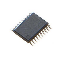
ATTINY861A-XU Atmel, ATTINY861A-XU Datasheet - Page 138

ATTINY861A-XU
Manufacturer Part Number
ATTINY861A-XU
Description
Microcontrollers (MCU) 8K Flash;125B EEPROM 128B SRAM;16 IO Pins
Manufacturer
Atmel
Datasheet
1.ATTINY861A-XU.pdf
(292 pages)
Specifications of ATTINY861A-XU
Core
RISC
Data Bus Width
8 bit
Program Memory Type
Flash
Program Memory Size
8 KB
Data Ram Size
512 B
Interface Type
SPI
Maximum Clock Frequency
20 MHz
Number Of Programmable I/os
16
Operating Supply Voltage
1.8 V to 5.5 V
Maximum Operating Temperature
+ 85 C
Mounting Style
SMD/SMT
Package / Case
TSSOP-20
Minimum Operating Temperature
- 40 C
Lead Free Status / Rohs Status
Details
Available stocks
Company
Part Number
Manufacturer
Quantity
Price
Company:
Part Number:
ATTINY861A-XUR
Manufacturer:
IDT
Quantity:
1 300
- Current page: 138 of 292
- Download datasheet (9Mb)
14.2.2
14.2.3
138
ATtiny261A/461A/861A
ACSRB – Analog Comparator Control and Status Register B
DIDR0 – Digital Input Disable Register 0
• Bits 1, 0 – ACIS1, ACIS0: Analog Comparator Interrupt Mode Select
These bits determine which comparator events that trigger the Analog Comparator interrupt. The
different settings are shown in
Table 14-2.
When changing the ACIS1/ACIS0 bits, the Analog Comparator Interrupt must be disabled by
clearing its Interrupt Enable bit in the ACSR Register. Otherwise an interrupt can occur when the
bits are changed.
• Bit 7 – HSEL: Hysteresis Select
When this bit is written logic one, the hysteresis of the Analog Comparator is switched on. The
hysteresis level is selected by the HLEV bit.
• Bit 6 – HLEV: Hysteresis Level
When the hysteresis is enabled by the HSEL bit, the Hysteresis Level, HLEV, bit selects the hys-
teresis level that is either 20mV (HLEV=0) or 50mV (HLEV=1).
• Bit 2:0 – ACM2:ACM0: Analog Comparator Multiplexer
The Analog Comparator multiplexer bits select the positive and negative input pins of the Analog
Comparator. The different settings are shown in
• Bits 7:4,2:0 – ADC6D:ADC0D: ADC6:0 Digital Input Disable
When this bit is written logic one, the digital input buffer on the corresponding ADC pin is dis-
abled. The corresponding PIN register bit will always read as zero when this bit is set. When an
analog signal is applied to the ADC7:0 pin and the digital input from this pin is not needed, this
bit should be written logic one to reduce power consumption in the digital input buffer.
• Bit 3 – AREFD: AREF Digital Input Disable
When this bit is written logic one, the digital input buffer on the AREF pin is disabled. The corre-
sponding PIN register bit will always read as zero when this bit is set. When an analog signal is
Bit
0x09 (0x29)
Read/Write
Initial Value
Bit
0x01 (0x21)
Read/Write
Initial Value
ACIS1
0
0
1
1
ACIS1/ACIS0 Settings
7
ADC6D
R/W
0
HSEL
R/W
7
0
ACIS0
0
1
0
1
6
ADC5D
R/W
0
HLEV
R/W
6
0
Interrupt Mode
Comparator Interrupt on Output Toggle.
Reserved
Comparator Interrupt on Falling Output Edge.
Comparator Interrupt on Rising Output Edge.
Table
5
ADC4D
R/W
0
N/A
R
5
-
14-2.
4
ADC3D
R/W
0
R
4
0
-
Table
3
AREFD
R/W
0
R
3
0
-
14-1.
2
ADC2D
R/W
0
ACM2
R/W
2
0
1
ADC1D
R/W
0
ACM1
R/W
1
0
0
ADC0D
0
R/W
ACM0
R/W
0
0
8197B–AVR–01/10
DIDR0
ACSRB
Related parts for ATTINY861A-XU
Image
Part Number
Description
Manufacturer
Datasheet
Request
R

Part Number:
Description:
DEV KIT FOR AVR/AVR32
Manufacturer:
Atmel
Datasheet:

Part Number:
Description:
INTERVAL AND WIPE/WASH WIPER CONTROL IC WITH DELAY
Manufacturer:
ATMEL Corporation
Datasheet:

Part Number:
Description:
Low-Voltage Voice-Switched IC for Hands-Free Operation
Manufacturer:
ATMEL Corporation
Datasheet:

Part Number:
Description:
MONOLITHIC INTEGRATED FEATUREPHONE CIRCUIT
Manufacturer:
ATMEL Corporation
Datasheet:

Part Number:
Description:
AM-FM Receiver IC U4255BM-M
Manufacturer:
ATMEL Corporation
Datasheet:

Part Number:
Description:
Monolithic Integrated Feature Phone Circuit
Manufacturer:
ATMEL Corporation
Datasheet:

Part Number:
Description:
Multistandard Video-IF and Quasi Parallel Sound Processing
Manufacturer:
ATMEL Corporation
Datasheet:

Part Number:
Description:
High-performance EE PLD
Manufacturer:
ATMEL Corporation
Datasheet:

Part Number:
Description:
8-bit Flash Microcontroller
Manufacturer:
ATMEL Corporation
Datasheet:

Part Number:
Description:
2-Wire Serial EEPROM
Manufacturer:
ATMEL Corporation
Datasheet:


