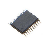
ATTINY861A-XU Atmel, ATTINY861A-XU Datasheet - Page 54

ATTINY861A-XU
Manufacturer Part Number
ATTINY861A-XU
Description
Microcontrollers (MCU) 8K Flash;125B EEPROM 128B SRAM;16 IO Pins
Manufacturer
Atmel
Datasheet
1.ATTINY861A-XU.pdf
(292 pages)
Specifications of ATTINY861A-XU
Core
RISC
Data Bus Width
8 bit
Program Memory Type
Flash
Program Memory Size
8 KB
Data Ram Size
512 B
Interface Type
SPI
Maximum Clock Frequency
20 MHz
Number Of Programmable I/os
16
Operating Supply Voltage
1.8 V to 5.5 V
Maximum Operating Temperature
+ 85 C
Mounting Style
SMD/SMT
Package / Case
TSSOP-20
Minimum Operating Temperature
- 40 C
Lead Free Status / Rohs Status
Details
Available stocks
Company
Part Number
Manufacturer
Quantity
Price
Company:
Part Number:
ATTINY861A-XUR
Manufacturer:
IDT
Quantity:
1 300
- Current page: 54 of 292
- Download datasheet (9Mb)
10.1
10.1.1
54
Ports as General Digital I/O
ATtiny261A/461A/861A
Configuring the Pin
The ports are bi-directional I/O ports with optional internal pull-ups.
tional description of one I/O-port pin, here generically called Pxn.
Figure 10-2. General Digital I/O
Note:
Each port pin consists of three register bits: DDxn, PORTxn, and PINxn. As shown in
Description” on page
at the PORTx I/O address, and the PINxn bits at the PINx I/O address.
The DDxn bit in the DDRx Register selects the direction of this pin. If DDxn is written logic one,
Pxn is configured as an output pin. If DDxn is written logic zero, Pxn is configured as an input
pin.
If PORTxn is written logic one when the pin is configured as an input pin, the pull-up resistor is
activated. To switch the pull-up resistor off, PORTxn has to be written logic zero or the pin has to
Pxn
1. WRx, WPx, WDx, RRx, RPx, and RDx are common to all pins within the same port. clk
SLEEP, and PUD are common to all ports.
PUD:
SLEEP:
clk
I/O
:
67, the DDxn bits are accessed at the DDRx I/O address, the PORTxn bits
PULLUP DISABLE
SLEEP CONTROL
I/O CLOCK
SLEEP
(1)
SYNCHRONIZER
D
L
Q
Q
D
PINxn
Q
Q
RESET
RESET
PORTxn
WDx:
RDx:
WRx:
RRx:
RPx:
WPx:
Q
Q
Q
Q
DDxn
CLR
CLR
D
D
RRx
WRITE DDRx
READ DDRx
WRITE PORTx
READ PORTx REGISTER
READ PORTx PIN
WRITE PINx REGISTER
Figure 10-2
PUD
WDx
RDx
RPx
clk
1
0
I/O
WRx
shows a func-
8197B–AVR–01/10
WPx
“Register
I/O
,
Related parts for ATTINY861A-XU
Image
Part Number
Description
Manufacturer
Datasheet
Request
R

Part Number:
Description:
DEV KIT FOR AVR/AVR32
Manufacturer:
Atmel
Datasheet:

Part Number:
Description:
INTERVAL AND WIPE/WASH WIPER CONTROL IC WITH DELAY
Manufacturer:
ATMEL Corporation
Datasheet:

Part Number:
Description:
Low-Voltage Voice-Switched IC for Hands-Free Operation
Manufacturer:
ATMEL Corporation
Datasheet:

Part Number:
Description:
MONOLITHIC INTEGRATED FEATUREPHONE CIRCUIT
Manufacturer:
ATMEL Corporation
Datasheet:

Part Number:
Description:
AM-FM Receiver IC U4255BM-M
Manufacturer:
ATMEL Corporation
Datasheet:

Part Number:
Description:
Monolithic Integrated Feature Phone Circuit
Manufacturer:
ATMEL Corporation
Datasheet:

Part Number:
Description:
Multistandard Video-IF and Quasi Parallel Sound Processing
Manufacturer:
ATMEL Corporation
Datasheet:

Part Number:
Description:
High-performance EE PLD
Manufacturer:
ATMEL Corporation
Datasheet:

Part Number:
Description:
8-bit Flash Microcontroller
Manufacturer:
ATMEL Corporation
Datasheet:

Part Number:
Description:
2-Wire Serial EEPROM
Manufacturer:
ATMEL Corporation
Datasheet:


