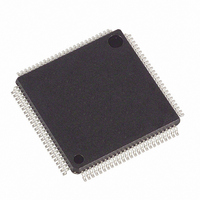
DS2156L+ Maxim Integrated Products, DS2156L+ Datasheet - Page 181

DS2156L+
Manufacturer Part Number
DS2156L+
Description
IC TXRX T1/E1/J1 1-CHIP 100-LQFP
Manufacturer
Maxim Integrated Products
Datasheet
1.DS2156L.pdf
(265 pages)
Specifications of DS2156L+
Function
Single-Chip Transceiver
Interface
E1, J1, T1, TDM, UTOPIA II
Number Of Circuits
1
Voltage - Supply
3.14 V ~ 3.47 V
Current - Supply
75mA
Operating Temperature
0°C ~ 70°C
Mounting Type
Surface Mount
Package / Case
100-LQFP
Includes
BERT Generator and Detector, CMI Coder and Decoder, HDLC Controller
Lead Free Status / RoHS Status
Lead free / RoHS Compliant
Power (watts)
-
- Current page: 181 of 265
- Download datasheet (2Mb)
An example for the receive direction is shown in Figure 24-11. The status signals UR-CLAVx are
associated to PHY port addresses #4, #3, #2, and #1. There is no need for a unique null device so “X =
don’t care” on the address lines UR-ADDRx.
In Figure 24-11, the polling of PHY ports starts while no cell transfer takes place. The ATM layer
monitors all four status signals UR-CLAVx. At clock edge #3 it detects a cell available at PHY port #1,
UR-CLAV(1) asserted. It selects that PHY port by placing address #1 on the address lines with rising
clock edge #3. PHY port #1 detects this at clock edge #4. At clock edge #5, PHY port #1 detects
UR-ENB asserted, thus cell transfer for PHY port #1 starts with rising clock edge #5.
At clock edge #5 the ATM layer detects a cell available at PHY port #3, UR-CLAV(3) asserted. Not
knowing whether PHY port #1 may have another cell available or not, the ATM layer deselects PHY port
#1 and selects PHY port #3 for cell transfer with rising clock edge #57 by placing address #3 on the
address lines and deasserting UR-ENB. PHY port #1 and PHY port #3 detect this at clock edge #58. At
clock edge #59, PHY port #3 detects UR-ENB asserted, thus cell transfer starts with rising clock edge
#59. At clock edge #111, no cell is available at PHY ports #1, #2, and #4. The ATM layer keeps
UR-ENB asserted and detects at clock edge #113 the first byte of another cell available from PHY port
#3, UR-CLAV(3) asserted. Thus, cell transfer takes place starting with rising clock edge #112. At clock
edge #164, again, no cell is available at PHY ports #1, #2, and #4. The ATM layer keeps the UR-ENB
asserted and also detects at clock edge #166 no cell available from PHY port #3, UR-CLAV(3)
deasserted. Thus, the ATM layer deselects PHY port #3 by deasserting UR-ENB with rising clock edge
#166.
Figure 24-11. Example of Direct Status Indication, Receive Direction
UR-CLAV(1)
UR-CLAV(2)
UR-CLAV(3)
UR-CLAV(4)
UR-ADDRx
UR-DATAx
UR-ENB
UR-CLK
UR-SOC
PORT #1
PORT #2
PORT #3
PORT #4
1
X
2
3
1
4
5
X
H1
Cell Transfer
6
(port #1)
57
P48
3
58
181 of 265
59
X
H1
Cell Transfer
60
(port #3)
111
P48
112
X
H1
113
Cell Transfer
(port #3)
H2
114
164
P48
165
X
166
X
167
Related parts for DS2156L+
Image
Part Number
Description
Manufacturer
Datasheet
Request
R

Part Number:
Description:
Ds2156, Ds2156l, Ds2156ln T1/e1/j1 Single-chip Transceiver Tdm/utopia Ii Interface
Manufacturer:
Maxim Integrated Products, Inc.
Datasheet:

Part Number:
Description:
MAX7528KCWPMaxim Integrated Products [CMOS Dual 8-Bit Buffered Multiplying DACs]
Manufacturer:
Maxim Integrated Products
Datasheet:

Part Number:
Description:
Single +5V, fully integrated, 1.25Gbps laser diode driver.
Manufacturer:
Maxim Integrated Products
Datasheet:

Part Number:
Description:
Single +5V, fully integrated, 155Mbps laser diode driver.
Manufacturer:
Maxim Integrated Products
Datasheet:

Part Number:
Description:
VRD11/VRD10, K8 Rev F 2/3/4-Phase PWM Controllers with Integrated Dual MOSFET Drivers
Manufacturer:
Maxim Integrated Products
Datasheet:

Part Number:
Description:
Highly Integrated Level 2 SMBus Battery Chargers
Manufacturer:
Maxim Integrated Products
Datasheet:

Part Number:
Description:
Current Monitor and Accumulator with Integrated Sense Resistor; ; Temperature Range: -40°C to +85°C
Manufacturer:
Maxim Integrated Products

Part Number:
Description:
TSSOP 14/A�/RS-485 Transceivers with Integrated 100O/120O Termination Resis
Manufacturer:
Maxim Integrated Products

Part Number:
Description:
TSSOP 14/A�/RS-485 Transceivers with Integrated 100O/120O Termination Resis
Manufacturer:
Maxim Integrated Products

Part Number:
Description:
QFN 16/A�/AC-DC and DC-DC Peak-Current-Mode Converters with Integrated Step
Manufacturer:
Maxim Integrated Products

Part Number:
Description:
TDFN/A/65V, 1A, 600KHZ, SYNCHRONOUS STEP-DOWN REGULATOR WITH INTEGRATED SWI
Manufacturer:
Maxim Integrated Products

Part Number:
Description:
Integrated Temperature Controller f
Manufacturer:
Maxim Integrated Products

Part Number:
Description:
SOT23-6/I�/45MHz to 650MHz, Integrated IF VCOs with Differential Output
Manufacturer:
Maxim Integrated Products

Part Number:
Description:
SOT23-6/I�/45MHz to 650MHz, Integrated IF VCOs with Differential Output
Manufacturer:
Maxim Integrated Products

Part Number:
Description:
EVALUATION KIT/2.4GHZ TO 2.5GHZ 802.11G/B RF TRANSCEIVER WITH INTEGRATED PA
Manufacturer:
Maxim Integrated Products


