SI3200-BS Silicon Laboratories Inc, SI3200-BS Datasheet - Page 17

SI3200-BS
Manufacturer Part Number
SI3200-BS
Description
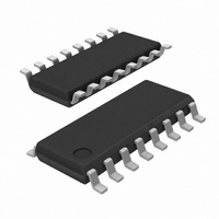
IC LINEFEED INTRFC 100V 16SOIC
Manufacturer
Silicon Laboratories Inc
Series
ProSLIC®r
Specifications of SI3200-BS
Function
Subscriber Line Interface Concept (SLIC), CODEC
Interface
GCI, PCM, SPI
Number Of Circuits
2
Voltage - Supply
3.3V, 5V
Current - Supply
110µA
Power (watts)
941mW
Operating Temperature
-40°C ~ 85°C
Mounting Type
Surface Mount
Package / Case
16-SOIC (3.9mm Width)
Includes
Battery Switching, BORSCHT Functions, DTMF Generation and Decoding, FSK Tone Generation, Modem and Fax Tone Detection
Lead Free Status / RoHS Status
Contains lead / RoHS non-compliant
Available stocks
Company
Part Number
Manufacturer
Quantity
Price
Company:
Part Number:
SI3200-BS
Manufacturer:
SILICON
Quantity:
1 082
Part Number:
SI3200-BS
Manufacturer:
N/A
Quantity:
20 000
Company:
Part Number:
SI3200-BSR
Manufacturer:
SILICON
Quantity:
14 000
Table 14. Switching Characteristics—GCI Highway Serial Interface
(V
Parameter
PCLK Period (2.048 MHz PCLK Mode)
PCLK Period (4.096 MHz PCLK Mode)
FSYNC Period
PCLK Duty Cycle Tolerance
FSYNC Jitter Tolerance
Rise Time, PCLK
Fall Time, PCLK
Delay Time, PCLK Rise to DTX Active
Delay Time, PCLK Rise to DTX Transition
Delay Time, PCLK Rise to DTX Tristate
Setup Time, FSYNC Rise to PCLK Fall
Hold Time, PCLK Fall to FSYNC Fall
Setup Time, DRX Transition to PCLK Fall
Hold Time, PCLK Falling to DRX Transition
FSYNC Pulse Width
Notes:
DD
1. All timing is referenced to the 50% level of the waveform. Input test levels are V
2. FSYNC source is assumed to be 8 kHz under all operating conditions.
3. Specification applies to PCLK fall to DTX tristate when that mode is selected.
, V
DD1
times are referenced to the 20% and 80% levels of the waveform.
–V
FSYNC
1
DD4
PCLK
Figure 3. GCI Highway Interface Timing Diagram (2.048 MHz PCLK Mode)
DRX
DTX
2
= 3.13 to 5.25 V, T
t
su1
Frame 0,
A
Bit 0
= 0 to 70 °C for K-Grade, –40 to 85 °C for B-Grade)
t
d1
3
Frame 0,
Symbol
Preliminary Rev. 0.91
t
Bit 0
h1
t
t
t
t
t
jitter
t
t
t
t
t
su1
su2
t
wfs
dty
t
t
d1
d2
d3
t
t
h1
h2
fs
p
p
r
f
t
Conditions
su2
t
d2
t
p
Test
t
h2
t
fs
Min
40
25
20
25
20
—
—
—
—
—
—
—
—
—
t
p
t
IH
r
= V
Si3220/Si3225
O
– 0.4 V, V
Typ
488
244
125
50
—
—
—
—
—
—
—
—
—
—
—
IL
= 0.4 V, rise and fall
t
f
±120
Max
t
d3
60
25
25
20
20
20
—
—
—
—
—
—
—
—
Units
µ s
ns
ns
ns
ns
ns
ns
ns
ns
ns
ns
ns
ns
ns
%
17


