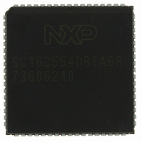
SC16C554DBIA68,529 NXP Semiconductors, SC16C554DBIA68,529 Datasheet - Page 55

SC16C554DBIA68,529
Manufacturer Part Number
SC16C554DBIA68,529
Description
IC UART QUAD W/FIFO 68-PLCC
Manufacturer
NXP Semiconductors
Type
Quad UART with 16-byte FIFOsr
Datasheet
1.SC16C554BIBS551.pdf
(58 pages)
Specifications of SC16C554DBIA68,529
Number Of Channels
4, QUART
Package / Case
68-LCC (J-Lead)
Features
Modem Control Function
Fifo's
16 Byte
Voltage - Supply
2.5V, 3.3V, 5V
With Auto Flow Control
Yes
With False Start Bit Detection
Yes
With Modem Control
Yes
With Cmos
Yes
Mounting Type
Surface Mount
Data Rate
5 Mbps
Supply Voltage (max)
5.5 V
Supply Voltage (min)
2.25 V
Supply Current
6 mA
Maximum Operating Temperature
+ 85 C
Minimum Operating Temperature
- 40 C
Mounting Style
SMD/SMT
Operating Supply Voltage
2.5 V or 3.3 V or 5 V
Lead Free Status / RoHS Status
Lead free / RoHS Compliant
Lead Free Status / RoHS Status
Lead free / RoHS Compliant, Lead free / RoHS Compliant
Other names
568-3269-5
935276668529
SC16C554DBIA68-S
935276668529
SC16C554DBIA68-S
Available stocks
Company
Part Number
Manufacturer
Quantity
Price
Company:
Part Number:
SC16C554DBIA68,529
Manufacturer:
NXP Semiconductors
Quantity:
10 000
NXP Semiconductors
14. Revision history
Table 30.
SC16C554B_554DB
Product data sheet
Document ID
SC16C554B_554DB v.4 20100608
Modifications:
SC16C554B_554DB_3
SC16C554B_554DB_2
(9397 750 14966)
SC16C554B_554DB_1
(9397 750 13133)
Revision history
Release date
20050901
20050613
20050209
•
•
•
•
•
•
•
•
•
The format of this data sheet has been redesigned to comply with the new identity guidelines
of NXP Semiconductors.
Legal texts have been adapted to the new company name where appropriate.
Section 2 “Features and
tolerant on input pins only”; added
Figure 9 “Autoflow control (auto-RTS and auto-CTS) example”
Table 24 “Limiting
– parameter description for symbol V
– symbol for ‘total power dissipation per package” changed from “P
Table 25 “Static
– symbol “V
– symbol “V
– parameter description for V
– symbol/parameter “I
– deleted (empty) Typ columns
Table 26 “Dynamic
– symbol “t
–
– added
Figure 23 “External clock
– symbol changed from “t
– symbol changed from “t
– symbol changed from “t
updated soldering information
other pin”; added separate conditions for “at D7 to D0” and “at any input only pin”
width HIGH” and “t
Table note
Table note [4]
All information provided in this document is subject to legal disclaimers.
1w
IL(CK)
IH(CK)
[2]: fraction’s denominator changed from “t
5 V, 3.3 V and 2.5 V quad UART, 5 Mbit/s (max.) with 16-byte FIFOs
, t
characteristics”:
2w
” changed to “V
values”:
” changed to “V
, clock pulse duration” is split to two symbols/parameters: “t
characteristics”:
Rev. 4 — 8 June 2010
WL
Data sheet status
Product data sheet
Product data sheet
Product data sheet
Product data sheet
CL
and its reference at t
, pulse width LOW”
benefits”: 7
, clock leakage” changed to “I
timing”:
2w
1w
3w
” to “t
” to “t
” to “t
OL
: moved “on all outputs” to Conditions column
IL(clk)
IH(clk)
WL
WH
w(clk)
Footnote
th
”
”
bullet item changed from “5 V tolerant inputs” to “5 V
n
”
”
”
changed from “voltage at any pin” to “voltage on any
1.
RESET
SC16C554B/554DB
L(clk)
Supersedes
SC16C554B_554DB_3
SC16C554B_554DB_2
SC16C554B_554DB_1
-
3w
” to “t
, clock leakage current”
updated
w(clk)
tot(pack)
”
© NXP B.V. 2010. All rights reserved.
” to “P
WH
, pulse
tot
/pack”
55 of 58


