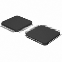
SC16C554IB80,557 NXP Semiconductors, SC16C554IB80,557 Datasheet - Page 23

SC16C554IB80,557
Manufacturer Part Number
SC16C554IB80,557
Description
IC UART QUAD SOT315-1
Manufacturer
NXP Semiconductors
Datasheet
1.SC16C554DIA68512.pdf
(55 pages)
Specifications of SC16C554IB80,557
Number Of Channels
4, QUART
Fifo's
16 Byte
Voltage - Supply
2.5V, 3.3V, 5V
With Auto Flow Control
Yes
With Irda Encoder/decoder
Yes
With False Start Bit Detection
Yes
With Modem Control
Yes
With Cmos
Yes
Mounting Type
Surface Mount
Package / Case
80-LQFP
Lead Free Status / RoHS Status
Lead free / RoHS Compliant
Other names
935270075557
SC16C554IB80
SC16C554IB80
SC16C554IB80
SC16C554IB80
Philips Semiconductors
9397 750 13132
Product data
7.1 Transmit (THR) and Receive (RHR) Holding Registers
7.2 Interrupt Enable Register (IER)
The serial transmitter section consists of an 8-bit Transmit Hold Register (THR) and
Transmit Shift Register (TSR). The status of the THR is provided in the Line Status
Register (LSR). Writing to the THR transfers the contents of the data bus (D7-D0) to
the THR, providing that the THR or TSR is empty. The THR empty flag in the LSR
register will be set to a logic 1 when the transmitter is empty or when data is
transferred to the TSR. Note that a write operation can be performed when the THR
empty flag is set (logic 0 = FIFO full; logic 1 = at least one FIFO location available).
The serial receive section also contains an 8-bit Receive Holding Register (RHR).
Receive data is removed from the SC16C554/554D and receive FIFO by reading the
RHR register. The receive section provides a mechanism to prevent false starts. On
the falling edge of a start or false start bit, an internal receiver counter starts counting
clocks at the 16 clock rate. After 7-
the center of the start bit. At this time the start bit is sampled, and if it is still a logic 0
it is validated. Evaluating the start bit in this manner prevents the receiver from
assembling a false character. Receiver status codes will be posted in the LSR.
The Interrupt Enable Register (IER) masks the interrupts from receiver ready,
transmitter empty, line status and modem status registers. These interrupts would
normally be seen on the INTA-INTD output pins in the 16 mode, or on wire-OR IRQ
output pin in the 68 mode.
Table 9:
Bit
7
6
5
4
3
Symbol
IER[7]
IER[6]
IER[5]
IER[4]
IER[3]
Interrupt Enable Register bits description
Quad UART with 16-byte FIFO and infrared (IrDA) encoder/decoder
Description
CTS interrupt.
RTS interrupt.
Xoff interrupt.
Sleep mode.
Modem Status Interrupt.
Logic 0 = Disable the CTS interrupt (normal default condition).
Logic 1 = Enable the CTS interrupt. The SC16C554/554D issues an
interrupt when the CTS pin transitions from a logic 0 to a logic 1.
Logic 0 = Disable the RTS interrupt (normal default condition).
Logic 1 = Enable the RTS interrupt. The SC16C554/554D issues an
interrupt when the RTS pin transitions from a logic 0 to a logic 1.
Logic 0 = Disable the software flow control, receive Xoff interrupt
(normal default condition).
Logic 1 = Enable the software flow control, receive Xoff interrupt. See
Section 6.7 “Software flow control”
Logic 0 = Disable sleep mode (normal default condition).
Logic 1 = Enable sleep mode. See
Logic 0 = Disable the modem status register interrupt (normal default
condition).
Logic 1 = Enable the modem status register interrupt.
Rev. 05 — 10 May 2004
1
2
clocks, the start bit time should be shifted to
Section 6.12 “Sleep mode”
for details.
SC16C554/554D
© Koninklijke Philips Electronics N.V. 2004. All rights reserved.
for details.
23 of 55


