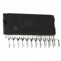
TDA8920CJ/N1,112 NXP Semiconductors, TDA8920CJ/N1,112 Datasheet - Page 20

TDA8920CJ/N1,112
Manufacturer Part Number
TDA8920CJ/N1,112
Description
IC AMP AUDIO PWR 220W 23SIL
Manufacturer
NXP Semiconductors
Type
Class Dr
Datasheet
1.TDA8920CJN1112.pdf
(39 pages)
Specifications of TDA8920CJ/N1,112
Output Type
1-Channel (Mono) or 2-Channel (Stereo)
Package / Case
23-SIL (Bent and Staggered Leads)
Max Output Power X Channels @ Load
220W x 1 @ 8 Ohm; 125W x 2 @ 4 Ohm
Voltage - Supply
±12.5 V ~ 32.5 V
Features
Depop, Differential Inputs, Mute, Short-Circuit and Thermal Protection, Standby
Mounting Type
Through Hole
Product
Class-D
Output Power
210 W
Available Set Gain
36 dB
Common Mode Rejection Ratio (min)
75 dB
Thd Plus Noise
0.05 %
Maximum Operating Temperature
+ 85 C
Mounting Style
Through Hole
Audio Load Resistance
8 Ohms
Dual Supply Voltage
+/- 30 V
Input Signal Type
Differential
Minimum Operating Temperature
- 40 C
Output Signal Type
Differential, Single
Supply Type
Dual
Lead Free Status / RoHS Status
Lead free / RoHS Compliant
Other names
568-4784-5
935281808112
TDA8920CJ/N1
TDA8920CJ/N1,112
TDA8920CJ/N1
935281808112
TDA8920CJ/N1
TDA8920CJ/N1,112
TDA8920CJ/N1
NXP Semiconductors
TDA8920C_2
Product data sheet
13.6 Pumping effects
In the following example, a heatsink calculation is made for an 8
When the maximum expected ambient temperature is 50 C, the total R
R
So the thermal resistance between heatsink and ambient temperature is:
The derating curves for power dissipation (for several R
Figure
maximum allowable power dissipation for a given heatsink size can be derived, or the
required heatsink size can be determined, at a required power dissipation level; see
Figure
In a typical stereo single-ended configuration, the TDA8920C is supplied by a symmetrical
supply voltage (e.g. V
configuration, a ‘pumping effect’ can occur. During one switching interval, energy is taken
from one supply (e.g. V
(e.g. V
across the output capacitors of that voltage supply source increases and the supply
voltage is pumped to higher levels. The voltage increase caused by the pumping effect
depends on:
Pumping effects should be minimized to prevent the malfunctioning of the audio amplifier
and/or the voltage supply source. Amplifier malfunction due to the pumping effect can
trigger UVP, OVP or UBP.
-------------------------
30 V supply:
148 50
•
•
•
•
•
th(j-a)
The audio signal has a crest factor of 10 (the ratio between peak power and average
power (20 dB)); this means that the average output power is
Thus, the peak RMS output power level is the 0.5 % THD level, i.e. 170 W.
The average power is then
The dissipated power at an output power of 17 W is approximately 7 W.
R
R
mounting)
R
th(j-c)
th(c-h)
th(h-a)
Speaker impedance
Supply voltage
Audio signal frequency
Value of supply line decoupling capacitors
Source and sink currents of other channels
7
–
SS
= R
9. A maximum junction temperature T
9.
(thermal resistance from junction to case) = 1.1 K/W
) and vice versa. When the voltage supply source cannot sink energy, the voltage
(thermal resistance from case to heatsink) = 0.5 K/W to 1 K/W (dependent on
(thermal resistance from heatsink to ambient) = 14
th(j-c)
=
14 K/W
+ R
th(c-h)
DD
Rev. 02 — 11 June 2009
DD
+ R
= 30 V and V
), while a part of that energy is returned to the other supply line
th(h-a)
1
10
170 W = 17 W.
SS
= 30 V). When the amplifier is used in an SE
j
= 150 C is taken into account. The
2
th(j-a)
110 W class-D power amplifier
values) are illustrated in
(1.1 + 1) = 11.9 K/W
1
10
of the peak power.
BTL application with a
TDA8920C
© NXP B.V. 2009. All rights reserved.
th(j-a)
becomes
20 of 39


