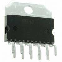
TDA7360 STMicroelectronics, TDA7360 Datasheet
TDA7360
Specifications of TDA7360
Available stocks


Related parts for TDA7360


TDA7360 Summary of contents
Page 1
... Loudspeaker protection – Overrating chip temperature – Load dump voltage – Fortuitous open ground – ESD Description The TDA7360 is a new technology class AB Audio Power Amplifier in the Multiwatt® package designed for car radio applications. Table 1. Device summary Order code ...
Page 2
... Reducing turn on-off pop . . . . . . . . . . . . . . . . . . . . . . . . . . . . . . . . . . . . . 23 4.2 Turn- 2/30 Polarization . . . . . . . . . . . . . . . . . . . . . . . . . . . . . . . . . . . . . . . . . . . . . . 15 SVR . . . . . . . . . . . . . . . . . . . . . . . . . . . . . . . . . . . . . . . . . . . . . . . . . . . . 15 Delayed turn-on (muting Stereo/bridge switching . . . . . . . . . . . . . . . . . . . . . . . . . . . . . . . . . . . . . 16 Standby . . . . . . . . . . . . . . . . . . . . . . . . . . . . . . . . . . . . . . . . . . . . . . . . . 16 Stability . . . . . . . . . . . . . . . . . . . . . . . . . . . . . . . . . . . . . . . . . . . . . . . . . 16 Clip detector . . . . . . . . . . . . . . . . . . . . . . . . . . . . . . . . . . . . . . . . . . . . . . 17 Output stage . . . . . . . . . . . . . . . . . . . . . . . . . . . . . . . . . . . . . . . . . . . . . 18 Amplifier block diagram . . . . . . . . . . . . . . . . . . . . . . . . . . . . . . . . . . . . . 19 Short circuit protection . . . . . . . . . . . . . . . . . . . . . . . . . . . . . . . . . . . . . . 20 Load dump voltage surge . . . . . . . . . . . . . . . . . . . . . . . . . . . . . . . . . . . 20 Polarity inversion . . . . . . . . . . . . . . . . . . . . . . . . . . . . . . . . . . . . . . . . . . 21 DC voltage . . . . . . . . . . . . . . . . . . . . . . . . . . . . . . . . . . . . . . . . . . . . . . . 21 Thermal shut-down . . . . . . . . . . . . . . . . . . . . . . . . . . . . . . . . . . . . . . . . 22 Loudspeaker protection . . . . . . . . . . . . . . . . . . . . . . . . . . . . . . . . . . . . . 22 Doc ID 1499 Rev 3 TDA7360 ...
Page 3
... TDA7360 4.3 Turn-off . . . . . . . . . . . . . . . . . . . . . . . . . . . . . . . . . . . . . . . . . . . . . . . . . . . 24 4.4 Global approach to solving pop problem by using the muting/turn-on delay function 25 4.5 Balance input in bridge configuration . . . . . . . . . . . . . . . . . . . . . . . . . . . . 27 5 Package information . . . . . . . . . . . . . . . . . . . . . . . . . . . . . . . . . . . . . . . . 28 6 Revision history . . . . . . . . . . . . . . . . . . . . . . . . . . . . . . . . . . . . . . . . . . . 29 Doc ID 1499 Rev 3 Contents 3/30 ...
Page 4
... List of tables List of tables Table 1. Device summary . . . . . . . . . . . . . . . . . . . . . . . . . . . . . . . . . . . . . . . . . . . . . . . . . . . . . . . . . . 1 Table 2. Absolute maximum ratings . . . . . . . . . . . . . . . . . . . . . . . . . . . . . . . . . . . . . . . . . . . . . . . . . . 8 Table 3. Thermal data Table 4. Electrical characteristics . . . . . . . . . . . . . . . . . . . . . . . . . . . . . . . . . . . . . . . . . . . . . . . . . . . . 8 Table 5. External components value of the stereo test and application circuits . . . . . . . . . . . . . . . . 10 Table 6. Document revision history . . . . . . . . . . . . . . . . . . . . . . . . . . . . . . . . . . . . . . . . . . . . . . . . . 29 4/30 Doc ID 1499 Rev 3 TDA7360 ...
Page 5
... TDA7360 List of figures Figure 1. Block diagram (stereo configuration Figure 2. Block diagram (bridge configuration Figure 3. Pins connection (top view Figure 4. Stereo test and application circuit . . . . . . . . . . . . . . . . . . . . . . . . . . . . . . . . . . . . . . . . . . . . 10 Figure 5. Printed circuit board of the stereo application circuit . . . . . . . . . . . . . . . . . . . . . . . . . . . . . 10 Figure 6. Bridge test and application circuit . . . . . . . . . . . . . . . . . . . . . . . . . . . . . . . . . . . . . . . . . . . . 11 Figure 7. Printed circuit board of the bridge application circuit . . . . . . . . . . . . . . . . . . . . . . . . . . . . . 11 Output power vs. supply voltage (Stereo, 4 Ω ...
Page 6
... Block and pins connection diagram 1 Block and pins connection diagram Figure 1. Block diagram (stereo configuration) Figure 2. Block diagram (bridge configuration) 6/30 Doc ID 1499 Rev 3 TDA7360 ...
Page 7
... TDA7360 Figure 3. Pins connection (top view) Block and pins connection diagram Doc ID 1499 Rev 3 7/30 ...
Page 8
... kHz unless otherwise specified. amb S Test condition - Stereo configuration - - Pin 2 pull with 10 kΩ 10% = 1.6 Ω Ω 3.2 Ω Ω Doc ID 1499 Rev 3 TDA7360 Value Unit -40 to 150 Value Unit Max. 1.8 °C/W Min. Typ. Max. Unit 120 mA 60 ...
Page 9
... TDA7360 Table 4. Electrical characteristics (continued) Symbol Parameter d Distortion SVR Supply voltage rejection C Crosstalk T R Input resistance I G Voltage gain V G Voltage gain match V E Input noise voltage IN Bridge V Output offset voltage OS P Output power o d Distortion SVR Supply voltage rejection R Input resistance ...
Page 10
... Larger than the recomm. Purpose value Input - Decoupling (CH1) Input Decoupling - (CH2) Supply voltage Rejection Longer turn-on delay time Filtering Capacitor Doc ID 1499 Rev 3 TDA7360 Smaller than the recomm.value - - – Worse supply voltage rejection. – Shorter turn-on delay time – DangEr Of Noise (POP) ...
Page 11
... TDA7360 Table 5. External components value of the stereo test and application circuits (continued) Component Recomm. value C4 22μF C5 220μF (min) C6 100nF (min) C7 2200μF Figure 6. Bridge test and application circuit Figure 7. Printed circuit board of the bridge application circuit Larger than the recomm. ...
Page 12
... Figure 10. Output power vs. supply voltage (Stereo, 3.2 Ω) Figure 12. Output power vs. supply voltage (Bridge, 3.2 Ω) 12/30 Figure 9. Output power vs. supply voltage (Stereo, 2 Ω) Figure 11. Output power vs. supply voltage (Bridge, 4 Ω) Figure 13. Drain current vs. supply voltage (Stereo) Doc ID 1499 Rev 3 TDA7360 ...
Page 13
... TDA7360 Figure 14. Distortion vs. output power (Stereo, 4 Ω) Figure 16. Distortion vs. output power (Stereo, 2 Ω) Figure 18. Distortion vs. output power (Bridge, 3.2 Ω) Figure 15. Distortion vs. output power (Stereo, 3.2 Ω) Figure 17. Distortion vs. output power (Bridge, 4 Ω) Figure 19. SVR vs. frequency and C3 (Stereo) Doc ID 1499 Rev 3 ...
Page 14
... Figure 24. Power dissipation and efficiency vs. output power (Bridge, 4 Ω) 14/30 Figure 21. Crosstalk vs. frequency (Stereo) Figure 23. Power dissipation and efficiency vs. output power (Stereo, 4 Ω) Figure 25. Power dissipation and efficiency vs. output power (Bridge, 3.2 Ω) Doc ID 1499 Rev 3 TDA7360 ...
Page 15
... Amplifier organization The TDA7360 has been developed taking care of the key concepts of the modern power audio amplifier for car radio such as: space and costs saving due to the minimized external count, excellent electrical performances, flexibility in use, superior reliability thanks to a built- in array of protections result the following performances has been achieved: – ...
Page 16
... The device is provided with an internal compensation which allows to reach low values of closed loop gain. In this way better performances on S/N ratio and SVR can be obtained. Figure 26. Turn-on delay circuit 16/30 26, 27, 28 and 2). A simple short circuit between two pins allows Doc ID 1499 Rev 3 TDA7360 ...
Page 17
... Figure 27. Mute function diagram 3.2.7 Clip detector The TDA7360 is equipped with an internal circuit able to detect the output stage saturation providing a proper current sinking into an open collector out. pin 2) when a certain distortion level is reached at each output. This particular function allows compression facility whenever the amplifier is over driven, so obtaining high quality sound at all listening levels ...
Page 18
... It is realized in a new bipolar technology, characterized by > 20V and BV > 50V both for NPN and PNP transistors. CBO Figure 33 has been chosen. First of all because its Doc ID 1499 Rev 3 vs. I CE(sat) C and cut-off frequency, is shown CEsat of the output transistors, which are in CEsat TDA7360 ...
Page 19
... TDA7360 It is possible, controlling the amount of this local feedback, to force the loop gain (A. β) to less than unity at frequencies for which the phase shift is 180°. This means that the output buffer is intrinsically stable and not prone to oscillation. Figure 33. The new output stage In contrast, with the circuit of frequencies is the use of an external RC network ...
Page 20
... Figure 36. Circuitry for short circuit detection 3.3.2 Load dump voltage surge The TDA7360 has a circuit which enables it to withstand a voltage pulse train on pin 9, of the type shown in Figure If the supply voltage peaks to more than 40V, then an LC filter must be inserted between the supply and pin 9, in order to assure that the pulses at pin 9 will be held within the limits shown ...
Page 21
... On the TDA7360 protection diodes are included to avoid any damage. 3.4.1 DC voltage The maximum operating DC voltage for the TDA7360 is 18V. However the device can withstand a DC voltage up to 28V with no damage. This could occur during winter if two batteries are series connected to crank the engine. Doc ID 1499 Rev 3 ...
Page 22
... Figure 39. Maximum allowable power dissipation vs. ambient temperature 3.4.3 Loudspeaker protection The TDA7360 guarantees safe operations even for the loudspeaker in case of accidental short-circuit. Whenever a single OUT to GND, OUT to V switched OFF so limiting dangerous DC current flowing through the loudspeaker. ...
Page 23
... This method can provide components and system cost saving. 4.1 Reducing turn on-off pop The TDA7360 has been designed in a way that the turn-on (off) transients are controlled through the charge (discharge) of the Csvr capacitor result of it, the turn-on (off) transient spectrum contents is limited only to the subsonic range ...
Page 24
... R out T > 170 ms with C = 2200μF, R out can become too high and a different approach may be useful (see svr show some types of electronic switches (μP compatible) suitable for Doc ID 1499 Rev 3 ) ext = 4 ohm, stereo ohm, stereo L ≤ 150 mV). CE TDA7360 ...
Page 25
... A simple approach to solving these problems is to use the mute characteristics of the TDA7360. If the SVR pin voltage below 1.5 V, the mute attenuation (typ) is 30dB.The amplifier is in play mode when V With the circuit of a time Toff after switch-off ...
Page 26
... Application hints Figure 44. Suggested muting circuit during amplifier switch-on and switch-off Figure 45. Timing diagram for the circuit depicted in fig. 44 Figure 46. Modification of the circuit depicted in fig.44 to drive two amplifiers 26/30 Doc ID 1499 Rev 3 TDA7360 ...
Page 27
... TDA7360 4.5 Balance input in bridge configuration A helpful characteristic of the TDA7360 is that, in bridge configuration, a signal present on both the input capacitors is amplified by the same amount and it is present in phase at the outputs, so this signal does not produce effects on the load.The typical value of CMRR is 46dB. ...
Page 28
... In order to meet environmental requirements, ST offers these devices in different grades of ® ECOPACK packages, depending on their level of environmental compliance. ECOPACK specifications, grade definitions and product status are available at: www.st.com. ® ECOPACK trademark. Figure 49. Multiwatt11 (vertical) mechanical data and package dimensions 28/30 Doc ID 1499 Rev 3 TDA7360 ® ...
Page 29
... TDA7360 6 Revision history Table 6. Document revision history Date 09-Jul-1997 20-Oct-1998 24-Feb-2011 Revision 1 Initial release. 2 Document status promoted from preliminary data to datasheet. Document reformatted. 3 Updated order code in Updated Section 5: Package Doc ID 1499 Rev 3 Revision history Changes Table 1: Device summary. information. 29/30 ...
Page 30
... Australia - Belgium - Brazil - Canada - China - Czech Republic - Finland - France - Germany - Hong Kong - India - Israel - Italy - Japan - Malaysia - Malta - Morocco - Philippines - Singapore - Spain - Sweden - Switzerland - United Kingdom - United States of America 30/30 Please Read Carefully: © 2011 STMicroelectronics - All rights reserved STMicroelectronics group of companies www.st.com Doc ID 1499 Rev 3 TDA7360 ...