TDA1910HS STMicroelectronics, TDA1910HS Datasheet - Page 11
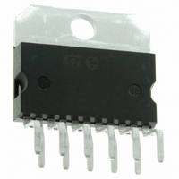
TDA1910HS
Manufacturer Part Number
TDA1910HS
Description
IC AMP AUD 10W MULTIWATT11 HORZ
Manufacturer
STMicroelectronics
Type
Class ABr
Datasheet
1.TDA1910HS.pdf
(15 pages)
Specifications of TDA1910HS
Output Type
1-Channel (Mono)
Max Output Power X Channels @ Load
17W x 1 @ 4 Ohm
Voltage - Supply
8 V ~ 30 V
Features
Depop, Mute, Thermal Protection
Mounting Type
Through Hole
Package / Case
Multiwatt-11 (Horizontal, Bent and Staggered Leads)
Operational Class
Class-AB
Audio Amplifier Output Configuration
1-Channel Mono
Output Power (typ)
17x1@4OhmW
Audio Amplifier Function
Speaker
Total Harmonic Distortion
0.2@8Ohm@7W%
Single Supply Voltage (typ)
9/12/15/18/24/28V
Dual Supply Voltage (typ)
Not RequiredV
Power Supply Requirement
Single
Power Dissipation
20W
Rail/rail I/o Type
No
Power Supply Rejection Ratio
60dB
Single Supply Voltage (min)
8V
Single Supply Voltage (max)
30V
Dual Supply Voltage (min)
Not RequiredV
Dual Supply Voltage (max)
Not RequiredV
Operating Temp Range
-40C to 150C
Operating Temperature Classification
Automotive
Mounting
Through Hole
Pin Count
11 +Tab
Package Type
MULTIWATT H
Lead Free Status / RoHS Status
Lead free / RoHS Compliant
Other names
497-8860-5
TDA1910HS
TDA1910HS
Available stocks
Company
Part Number
Manufacturer
Quantity
Price


APPLICATION SUGGESTION
The recommended values of the components are those shown on application circuit of fig. 21. Different
values can be used.
The following table can help the designer.
Component
R
g
R
R
R
C
C
C
C
C
C
C
C
C
P
+ R
2
3
4
1
1
2
3
4
5
6
7
8
9
1
Raccom.
(R
(R
1000 F
2200 F
0.22 F
0.22 F
3.3K
value
10K
20K
2.2 F
0.1 F
100
10 F
47 F
L
L
1 F
1 F
1
= 4 )
= 8 )
Input signal imped.
for muting operation
Close loop gain
setting.
Close loop gain
setting.
Frequency stability
Volume
potentiometer.
Input DC decoupling.
Inverting input DC
decoupling.
Supply voltage
bypass.
Ripple rejection.
Bootstrap.
Frequency stability.
Output DC
decoupling.
Purpose
recommended value
Increase of the atte-
nuation in muting-on
condition. Decrease
of the input sensitivity.
Increase of gain.
Decrease of gain.
Danger of oscillation
at high frequencies
with inductive loads.
Increase of the
switch-on noise.
Increase of the
switch-on noise.
Increase of SVR.
Increase of the
switch-on time
Larger than
recommended value
Decrease of gain.
Increase of gain.
Decrease of the
attenuation in muting
on condition.
Increase quiescent
current.
Decrease of the input
impedance and of the
input level.
Higher low frequency
cutoff.
Higher low frequency
cutoff.
Danger of oscillations.
Degradation of
SVR
Increase of the distor-
tion at low frequency.
Danger of oscillation.
Higher low frequency
cutoff.
Smaller than
10K
0.1 F
2.2 F
10 F
Allowed range
Min.
9 R
3
TDA1910
100K
100 F
100 F
Max.
R
2
11/15
/9
Related parts for TDA1910HS
Image
Part Number
Description
Manufacturer
Datasheet
Request
R

Part Number:
Description:
STMicroelectronics [RIPPLE-CARRY BINARY COUNTER/DIVIDERS]
Manufacturer:
STMicroelectronics
Datasheet:
Part Number:
Description:
STMicroelectronics [LIQUID-CRYSTAL DISPLAY DRIVERS]
Manufacturer:
STMicroelectronics
Datasheet:

Part Number:
Description:
BOARD EVAL FOR MEMS SENSORS
Manufacturer:
STMicroelectronics
Datasheet:
Part Number:
Description:
NPN TRANSISTOR POWER MODULE
Manufacturer:
STMicroelectronics
Datasheet:
Part Number:
Description:
TURBOSWITCH ULTRA-FAST HIGH VOLTAGE DIODE
Manufacturer:
STMicroelectronics
Datasheet:
Part Number:
Description:
Manufacturer:
STMicroelectronics
Datasheet:
Part Number:
Description:
DIODE / SCR MODULE
Manufacturer:
STMicroelectronics
Datasheet:
Part Number:
Description:
DIODE / SCR MODULE
Manufacturer:
STMicroelectronics
Datasheet:
Part Number:
Description:
Search -----> STE16N100
Manufacturer:
STMicroelectronics
Datasheet:
Part Number:
Description:
Search ---> STE53NA50
Manufacturer:
STMicroelectronics
Datasheet:
Part Number:
Description:
NPN Transistor Power Module
Manufacturer:
STMicroelectronics
Datasheet:
Part Number:
Description:
DIODE / SCR MODULE
Manufacturer:
STMicroelectronics
Datasheet: