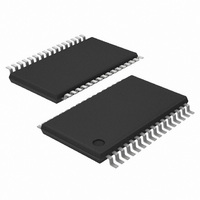
TDA8933BTW/N2,518 NXP Semiconductors, TDA8933BTW/N2,518 Datasheet - Page 27

TDA8933BTW/N2,518
Manufacturer Part Number
TDA8933BTW/N2,518
Description
IC AMP AUDIO 20.6W STER 32TSSOP
Manufacturer
NXP Semiconductors
Type
Class Dr
Datasheet
1.TDA8933BTWN2118.pdf
(42 pages)
Specifications of TDA8933BTW/N2,518
Output Type
1-Channel (Mono) or 2-Channel (Stereo)
Max Output Power X Channels @ Load
20.6W x 1 @ 16 Ohm; 10.3W x 2 @ 8 Ohm
Voltage - Supply
10 V ~ 36 V, ±5 V ~ 18 V
Features
Depop, Differential Inputs, Mute, Short-Circuit and Thermal Protection
Mounting Type
Surface Mount
Package / Case
32-TSSOP Exposed Pad, 32-eTSSOP, 32-HTSSOP
Lead Free Status / RoHS Status
Lead free / RoHS Compliant
Other names
935285222518
TDA8933BTW/N2-T
TDA8933BTW/N2-T
TDA8933BTW/N2-T
TDA8933BTW/N2-T
NXP Semiconductors
TDA8933B_1
Preliminary data sheet
14.7 Thermal behavior (PCB considerations)
14.8 Pumping effects
The TDA8933B is available in a thermally enhanced HTSSOP32 (SOT549-1) package for
reflow soldering.
The HTSSOP32 package has an exposed die pad that reduces significantly the overall
Rth(j-a). Therefore it is required to solder the exposed die pad (at VSSD level) to a copper
plane for cooling. A low thermal-resistance can be achieved when using a multilayer PCB
with sufficient space for two or three thermal planes. Increasing the area of the thermal
plane, the number of planes or the copper thickness can reduce further the thermal
resistance R
Find below the typical thermal resistance (free air and natural convection) of two practical
PCB implementations:
Equation 10
the thermal resistance from junction to ambient.
Where:
The power dissipation is shown in
Thermal foldback will limit the maximum junction temperature to 140 C.
When the amplifier is used in an SE configuration a so-called ‘pumping effect’ can occur.
During one switching interval, energy is taken from one supply (e.g. V
that energy is delivered back to the other supply line (e.g. V
the power supply cannot sink energy the voltage across output capacitors that power
supply will increase.
The voltage increase caused by the pumping effect depends on:
R
•
•
•
•
•
•
•
•
•
•
•
th j a
R
FR4 base material).
R
FR4 base material).
R
T
T
P = power dissipation, which is determined by the efficiency of the TDA8933B
Speaker impedance
Supply voltage
Audio signal frequency
Value of decoupling capacitors on supply lines
Source and sink currents of other channels
–
j(max)
amb
th(j-a)
th(j-a)
th(j-a)
=
= ambient temperature ( C)
= 48 K/W for a small two-layer application board (55 mm
= 30 K/W for a three-layer application board (70 mm
= thermal resistance from junction to ambient (K/W)
= maximum junction temperature ( C)
T
----------------------------------- -
th(j-a)
shows the relation between the maximum allowable power dissipation P and
j max
of both packages.
P
–
T
Rev. 01 — 23 October 2008
amb
Figure 19
(SE) and
Figure 27
SSP1
) and vice versa. When
Class D audio amplifier
(BTL).
50 mm, 35 m copper,
TDA8933B
DDP1
40 mm, m copper,
© NXP B.V. 2008. All rights reserved.
), while a part of
27 of 42
(10)


