STA540 STMicroelectronics, STA540 Datasheet
STA540
Specifications of STA540
Available stocks


Related parts for STA540


STA540 Summary of contents
Page 1
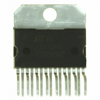
... Order code STA540 -40 to 150° C January 2008 dual/quad power amplifier Description The STA540 is a 4-channel, class AB audio amplifier designed for high quality sound applications. The amplifiers have single-ended outputs with integrated short-circuit protection, thermal protection and diagnostic functions. The chip is housed in the 15-pin Multiwatt ECOPACK (2002/95/EC) compliant ...
Page 2
... R calculation for 4 single-ended channels . . . . . . . . . . . . . . . . . . . 13 th_HS R calculation for 2 single-ended channels plus 1 BTL channel . . . 13 th_HS Calculations using music power . . . . . . . . . . . . . . . . . . . . . . . . . . . . . . . 14 Rail-to-rail output voltage swing without bootstrap capacitors . . . . . . . . 16 Absolute stability without external compensation . . . . . . . . . . . . . . . . . 16 Diagnostic facilities (pin 10 Short-circuit protection . . . . . . . . . . . . . . . . . . . . . . . . . . . . . . . . . . . . . . 17 Clipping detection . . . . . . . . . . . . . . . . . . . . . . . . . . . . . . . . . . . . . . . . . 18 Thermal shutdown . . . . . . . . . . . . . . . . . . . . . . . . . . . . . . . . . . . . . . . . . 18 STA540 ...
Page 3
... STA540 6.8 Handling the diagnostic information . . . . . . . . . . . . . . . . . . . . . . . . . . . . . 19 6.9 PCB ground layout . . . . . . . . . . . . . . . . . . . . . . . . . . . . . . . . . . . . . . . . . . 20 6.10 Mute function . . . . . . . . . . . . . . . . . . . . . . . . . . . . . . . . . . . . . . . . . . . . . . 20 7 Package information . . . . . . . . . . . . . . . . . . . . . . . . . . . . . . . . . . . . . . . . 21 8 Revision history . . . . . . . . . . . . . . . . . . . . . . . . . . . . . . . . . . . . . . . . . . . 22 Contents 3/23 ...
Page 4
... Block diagram and pin description 1 Block diagram and pin description 1.1 Block diagram Figure 1. Block diagram ST-BY ST-BY 4/23 VCC2 VCC1 V V CC2 CC1 IN1 A2 INV 7 5 IN2 12 IN3 A4 INV 11 IN4 6 SVR OUT1 - + 2 OUT2 - OUT3 - + 14 OUT4 - DIAGNOSTIC 10 DIAGNOSTICD OUTPUT 8 9 P-GND S-GND D06AU1630 STA540 ...
Page 5
... STA540 1.2 Pin description Figure 2. Pin connection (top view) Table 2. Pin description N° Name ST-BY 8 P-GND 9 S-GND 10 DIAGNOSTICD Type OUT1 OUT Channel 1 output OUT2 OUT Channel 2 output VCC1 PWR Power supply IN1 IN Channel 1 input IN2 IN Channel 2 input SVR IN Supply voltage rejection ...
Page 6
... THD=10%, R THD=10%, R THD=10%, R THD=10%, R THD=10%, R THD=10 Ω Value -40 to150 Value 1 25° C unless otherwise amb Min Typ 8 80 -150 =4 Ω 6.5 =2 Ω 11 Ω Ω Ω Ω 0.02 4.0 STA540 Unit °C °C Unit °C/W °C/W Max Unit 22 V 150 mA 150 ...
Page 7
... STA540 Table 5. Electrical characteristics (continued) Symbol C Crosstalk T R Input impedance in G Voltage gain v G Voltage gain match v E Input noise voltage N SVR Supply voltage rejection A Standby attenuation SB Current consumption standby Pin ST-BY voltage for play V Pin ST-BY voltage for ST-BY standby ...
Page 8
... Suggested applications into 2 Ω 1000 µ into 4 Ω into 2 Ω into 4 Ω OUT_1 into 4 Ω OUT_2 OUT_3 OUT_4 470µF S uggested applications into 4 Ω kHz, 10% THD into 8 Ω kHz, 10% THD into 4 Ω kHz, 10% THD into 8 Ω kHz, 10% THD OUT_L STA540 ...
Page 9
... Figure 6. Stereo plus bridge drive ST_BY IN_L IN_R IN_Bridge 10 kΩ 100 nF 10 µ 220 nF 2200 µ STA540 220 nF 2200 µ 470 µF Suggested applications into 2 Ω, + into 4 Ω into 2 Ω, + into 4 Ω into 4 Ω, + into 8 Ω Standard application circuits ...
Page 10
... Output power versus supply voltage Figure 10. Output power versus supply voltage Po ( SINGLE ENDED RL= 2 Ω KHz (V) Figure 11. Output power versus supply voltage Figure 12. Distortion versus output power 10/23 Figure THD THD Quiescent output voltage versus supply voltage (single-ended and bridge) SINGLE ENDED THD RL= 4Ω KHz THD (V) STA540 17 18 ...
Page 11
... STA540 Figure 13. Distortion versus output power Figure 15. Output power versus supply voltage Figure 16. Output power versus supply voltage 12 12 Po S.E. S. Rl=8ohm Rl=8ohm 9 9 f=1KHz f=1KHz T.H.D=10% T.H.D=10 +10 +10 +12 +12 +14 +14 +16 +16 Vs(V) Vs(V) Figure 17. Supply voltage rejection versus frequency Figure 14. Distortion versus output power ...
Page 12
... Electrical characteristics curves Figure 19. Standby attenuation versus threshold voltage Figure 21. Total power dissipation and efficiency versus output power 12/23 Figure 20. Total power dissipation and efficiency versus output power STA540 ...
Page 13
... STA540 5 Thermal information In order to avoid the intervention of the thermal protection, placed at T muting and T =160° C for thermal shutdown important to calculate the heatsink thermal j resistance, R th_HS The parameters that influence the calculation are: " maximum dissipated power for the device (P " ...
Page 14
... When music power is considered the resulting dissipation is about 40% less than the calculated maximum. Thus, smaller or cheaper heatsinks can be employed. The heatsink thermal resistance values are modified as follows: for example 5.1.1: 10 40% = 6.3 W, thus giving R for example 5.1. 40% = 12.6 W, thus giving R 14/23 STA540 = 14° C/W, th_c-amb = 6° C/W. th_c-amb ...
Page 15
... STA540 6 Practical information 6.1 Highly flexible amplifier configuration The availability of four independent channels makes it possible to accomplish several kinds of applications ranging from four speakers stereo (F/R) to two-speaker bridge solutions. When working with single-ended configurations, the polarity of the speakers driven by the inverting amplifier must be reversed with respect to those driven by non-inverting channels. ...
Page 16
... This contrasts with the classical PNP-NPN stage which makes use of external RC networks, namely the Boucherot cells, for reducing the gain at high frequencies. Figure 22. The new output stage 16/23 of the output transistors, which are in the CEsat ) each. sat Figure 22, the low frequency gain V STA540 Figure 22 and allows the full /V is greater out in ...
Page 17
... STA540 6.7 Built–in protection 6.7.1 Diagnostic facilities (pin 10) The STA540 is equipped with diagnostic circuitry that is able to detect the following events: " clipping of the output signal, " thermal shutdown, " output fault: – short circuit to GND, – short circuit to VS, – ...
Page 18
... C before the shutdown temperature is reached. Figure 25. Output fault waveforms (see Figure 26. Fault waveforms ST-BY PIN VOLTAGE OUTPUT WAVEFORM Vpin 10 18/23 Figure 2V OUT TO Vs SHORT SOFT SHORT OUT TO GND SHORT CORRECT TURN-ON FAULT DETECTION CHECK AT TURN-ON D05AU1603mod (TEST PHASE) 26 SHORT TO GND STA540 ...
Page 19
... STA540 6.8 Handling the diagnostic information As different diagnostic information (clipping detection, output fault, approaching thermal shutdown) becomes available at pin 10 so the behavior of the signal at this pin changes. In order to discriminate the event, signal DIAGNOSTICD, pin 10, must be interpreted correctly. Figure 27 corresponding output on pin 10. ...
Page 20
... ST-BY 10µF 0.22µ 0.22µ 0.47µF IN BRIDGE 3.3K MUTE 470µF R2 10K V S 100nF 1000µ OUT L 2200µF 2 OUT R 2200µF 15 OUT BRIDGE DIAGNOSTICS D06AU1632 STA540 Figure 29. ...
Page 21
... STA540 7 Package information In order to meet environmental requirements, ST offers these devices in ECOPACK packages. These packages have a Lead-free second level interconnect. The category of second Level Interconnect is marked on the package and on the inner box label, in compliance with JEDEC Standard JESD97. The maximum ratings related to soldering conditions are also marked on the inner box label ...
Page 22
... Document revision history Date 21-Jan-2008 Oct-2007 Sep-2006 May-2006 22/23 Revision Updated power specifications on pages 1, 6 and 8 4 Updated short-circuit output current in Table 5 Updated description on page 1 3 Updated pin naming, numbering in all relevant figures Minor non-technical edits 2 Minor non-technical edits 1 Initial release STA540 Changes ...
Page 23
... STA540 Information in this document is provided solely in connection with ST products. STMicroelectronics NV and its subsidiaries (“ST”) reserve the right to make changes, corrections, modifications or improvements, to this document, and the products and services described herein at any time, without notice. All ST products are sold pursuant to ST’s terms and conditions of sale. ...