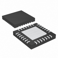
MAX9850ETI+T Maxim Integrated Products, MAX9850ETI+T Datasheet - Page 28

MAX9850ETI+T
Manufacturer Part Number
MAX9850ETI+T
Description
IC AMP AUDIO .095W STER 28TQFN
Manufacturer
Maxim Integrated Products
Series
DirectDrive™r
Type
Class ABr
Datasheet
1.MAX9850ETI.pdf
(36 pages)
Specifications of MAX9850ETI+T
Output Type
Headphones, 2-Channel (Stereo)
Max Output Power X Channels @ Load
95mW x 2 @ 16 Ohm
Voltage - Supply
1.8 V ~ 3.6 V
Features
DAC, Depop, Digital Inputs, I²C, I²S, Line Level Inputs & Outputs, Mute, Shutdown, Volume Control
Mounting Type
Surface Mount
Package / Case
28-WQFN Exposed Pad, 28-HWQFN
Lead Free Status / RoHS Status
Lead free / RoHS Compliant
1 = Accepts audio data LSB first.
0 = Accepts audio data MSB first.
Set LSF = 0 to conform to the I
1 = Audio data is latched into the MAX9850 on the sec-
ond rising BCLK edge after LRCLK transitions.
0 = Audio data is latched into the MAX9850 on the first
rising BCLK edge after LRCLK transitions
Set DLY = 1 to conform to the I
1 = Audio data is right justified.
0 = Audio data is left justified.
I
I
00 = Audio data word length is 16 bits.
01 = Audio data word length is 18 bits.
10 = Audio data word length is 20 bits.
11 = Audio data word length is 24 bits.
Program WS(1:0) to select the input data word length.
Programming the audio data word length ensures that
the correct number of BCLK cycles are output to
accommodate the incoming data word.
The MAX9850 receives serial digital audio data through a
3-wire interface. The data can be right or left justified,
MSB or LSB first, or I
carries two time-multiplexed audio data channels (SDIN),
a channel-select line (LRCLK), and a bit clock line
(BCLK). The configuration of the audio interface is con-
trolled with the digital audio register, see Table 20.
Typical digital audio formats, and the required digital
audio register code, are listed in Table 21. Figure 4 illus-
trates the difference between right justified, left justified,
and I
The MAX9850 generates the BCLK and the LRCLK from
ICLK when in master mode, see the Internal Timing sec-
tion. In slave mode, the MAX9850 accepts an LRCLK and
BCLK from an external digital audio source.
Stereo Audio DAC with DirectDrive
Headphone Amplifier
Table 21. Typical Digital Audio Formats
28
2
2
Left-Justified Audio Data
Right-Justified Audio Data
I
2
S data is left justified. Set RTJ = 0 to conform to the
S standard.
S-Compatible Audio Data
2
______________________________________________________________________________________
S compatible audio data.
FORMAT
2
S compatible. The 3-wire serial bus
Least Significant Bit First (LSF)
Word Length Select (WS(1:0))
Digital Audio Interface
Right-Justified Data (RTJ)
DIGITAL AUDIO REGISTER
2
2
S standard.
S standard.
SDIN Delay (DLY)
CODE (0xA)
X0000000
X0000100
X0001000
The MAX9850 can accept right- or left-justified data when
operating in slave mode with extra BCLK pulses beyond
what is programmed by the WS(1:0) bits. When using the
I
the second BCLK rising edge following an LRCLK transi-
tion. See Figure 4 for the various relationships between
clock and data that are supported by the MAX9850.
The MAX9850 can be configured to accept 16, 18, 20,
or 24-bit data. The MAX9850 generates exactly the pro-
grammed number of BCLK cycles when in master
mode. Program the audio data word size with WS(1:0)
(register 0xA, bit B0 and B1) according to Table 22 to
ensure that the MAX9850 outputs the correct number of
BCLK cycles to accommodate the input word.
The internal digital processing resolution is 18 bits
wide. Data words longer than 18 bits will be truncated.
Zeros are internally programmed into the missing bit
positions when the data word is shorter than the pro-
grammed word size.
The MAX9850 features an I
wire serial interface consisting of a serial data line
(SDA) and a serial clock line (SCL). SDA and SCL facili-
tate communication between the MAX9850 and the
master at clock rates up to 400kHz. Figure 5 shows the
2-wire interface timing diagram. The master generates
SCL and initiates data transfer on the bus.
A master device writes data to the MAX9850 by trans-
mitting the proper slave address followed by the regis-
ter address and then the data word. Each transmit
sequence is framed by a START (S) or REPEATED
START (Sr) condition and a STOP (P) condition. Each
word transmitted to the MAX9850 is 8 bits long and is
followed by an acknowledge clock pulse.
Table 22. Audio Data Word Size
SMBus is a trademark of Intel Corp.
2
S standard, audio data MSBit must latch into SDIN on
WS(1:0)
0x0
0x1
0x2
0x3
I
2
C-Compatible Serial Interface
2
C/SMBus™-compatible, 2-
DATA WORD SIZE (BITS)
16
18
20
24


