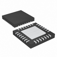
MAX9850ETI+T Maxim Integrated Products, MAX9850ETI+T Datasheet - Page 34

MAX9850ETI+T
Manufacturer Part Number
MAX9850ETI+T
Description
IC AMP AUDIO .095W STER 28TQFN
Manufacturer
Maxim Integrated Products
Series
DirectDrive™r
Type
Class ABr
Datasheet
1.MAX9850ETI.pdf
(36 pages)
Specifications of MAX9850ETI+T
Output Type
Headphones, 2-Channel (Stereo)
Max Output Power X Channels @ Load
95mW x 2 @ 16 Ohm
Voltage - Supply
1.8 V ~ 3.6 V
Features
DAC, Depop, Digital Inputs, I²C, I²S, Line Level Inputs & Outputs, Mute, Shutdown, Volume Control
Mounting Type
Surface Mount
Package / Case
28-WQFN Exposed Pad, 28-HWQFN
Lead Free Status / RoHS Status
Lead free / RoHS Compliant
The MAX9850 is a complete cell-phone audio playback
solution. In a typical application, ringtones are created
and output through the application’s processor on the
digital audio bus. Connect the baseband IC to the line
inputs of the MAX9850, INR and INL. The headphone
amplifier outputs a summed version of the digital audio
input and the line input (see Figure 13).
The headphone amplifiers can provide almost ±300mA
per channel during a short-circuit event. The MAX9850
has been designed to withstand this current continu-
ously. To avoid unnecessarily draining a battery, it is
advised to enable the IOHR and IOHL hardware inter-
rupt. The µC can service the interrupt by disabling the
headphone amplifiers and waiting for a timeout period.
A headphone short-circuit event on the right channel
only may also indicate that a mono headphone has
been inserted into the stereo socket. The µC can then
automatically disable the right channel by placing the
MAX9850 in mono mode. This resolves a mono jack-
induced, short-circuit condition.
Stereo Audio DAC with DirectDrive
Headphone Amplifier
Figure 13. Cell Phone Audio
34
______________________________________________________________________________________
BASEBAND
APPLICATIONS
PROCESSOR
IC
0.47μF
0.47μF
Headphone Short Circuit
1μF
INL
INR
SCL
SDA
MCLK
SDIN
BCLK
LRCLK
PV
SS
DV
2.2μF
DD
1μF
SV
Cell Phone Audio
SS
1.8V TO 3.6V
MAX9850
PGND
PV
DD
1μF
DGND
AV
DD
AGND
OUTR
OUTL
GPIO
C1P
C1N
HPL
HPS
HPR
REF
0.47μF
Proper layout and grounding are essential for optimum
performance. Use large traces for the power-supply
inputs and amplifier outputs to minimize losses due to
parasitic trace resistance. Large traces also aid in moving
heat away from the package. Proper grounding improves
audio performance, minimizes crosstalk between chan-
nels, and prevents any switching noise from coupling into
the audio signal. Connect PGND, DGND, and AGND
together at a single point on the PC board. Route DGND,
PGND, and all traces that carry switching transients or
digital signals away from AGND and traces or compo-
nents in the analog audio-signal path.
Connect all components associated with the charge
pump to PGND. Connect PV
the device. Place the charge-pump capacitors as close
to PV
Bypass PV
capacitors as close to the device as possible.
The MAX9850 thin QFN package features an exposed
thermal pad on its underside. This pad lowers the pack-
age’s thermal resistance by providing a direct heat con-
duction path from the die to the printed circuit board. If
possible, connect the exposed thermal pad to an electri-
cally isolated, large pad of copper. If it cannot be left
floating, connect it to AGND.
SS
1μF
as possible. Ensure C2 is connected to PGND.
DV
DD
DD
10kΩ
0.47μF
0.47μF
PC Board Layout and Bypassing
*FUTURE PRODUCT—CONTACT FACTORY FOR AVAILABILITY.
with 1µF to PGND. Place the bypass
0.47μF
0.47μF
INL+
INL-
INR+
INR-
SHDN
MAX9701*
3.3V TO 5.5V
SS
V
DD
and SV
PGND
OUTR+
OUTR-
OUTL+
OUTL-
SS
together at


