TDA8946AJ/N2,112 NXP Semiconductors, TDA8946AJ/N2,112 Datasheet - Page 6
TDA8946AJ/N2,112
Manufacturer Part Number
TDA8946AJ/N2,112
Description
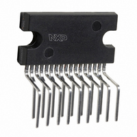
IC AMP AUDIO PWR 15W STER 17SIL
Manufacturer
NXP Semiconductors
Type
Class ABr
Datasheet
1.TDA8946AJN2112.pdf
(20 pages)
Specifications of TDA8946AJ/N2,112
Output Type
2-Channel (Stereo)
Package / Case
17-SIL (Bent and Staggered Leads)
Max Output Power X Channels @ Load
15W x 2 @ 8 Ohm
Voltage - Supply
4.5 V ~ 18 V
Features
Depop, Mute, Short-Circuit and Thermal Protection, Standby
Mounting Type
Through Hole
Product
Class-AB
Output Power
15 W
Available Set Gain
30 dB
Thd Plus Noise
0.07 %
Operating Supply Voltage
18 V
Maximum Power Dissipation
28000 mW
Maximum Operating Temperature
+ 85 C
Mounting Style
SMD/SMT
Audio Load Resistance
8 Ohms
Input Signal Type
Differential
Minimum Operating Temperature
- 40 C
Output Signal Type
Differential
Supply Type
Single
Supply Voltage (max)
18 V
Supply Voltage (min)
4.5 V
Lead Free Status / RoHS Status
Lead free / RoHS Compliant
Other names
568-3456-5
935270283112
TDA8946AJU
935270283112
TDA8946AJU


Philips Semiconductors
9397 750 09434
Product data
8.3.1 Switch-on and switch off
8.3 Mode selection
8.4 DC gain control
8.5 Supply Voltage Ripple Rejection (SVRR)
Table 4:
For the average listening level a power dissipation of 8.5 W can be used for a
heatsink calculation.
The TDA8946AJ has three functional modes, which can be selected by applying the
proper DC voltage to pin MODE.
Standby — In this mode the current consumption is very low and the outputs are
floating. The device is in standby mode when V
MODE pin is left floating.
Mute — In this mode the amplifier is DC-biased but not operational (no audio output).
This allows the input coupling capacitors to be charged to avoid pop-noise. The
device is in mute mode when 3.5 V < V
Operating — In this mode the amplifier is operating normally. The operating mode is
activated at V
To avoid audible plops during supply voltage switch-on or switch-off, the device is set
to standby mode before the supply voltage is applied (switch-on) or removed
(switch-off).
The switch-on and switch-off time can be influenced by an RC-circuit on the MODE
pin. Rapid on/off switching of the device or the rapid switching of the MODE pin may
cause ‘click-and pop-noise’. This can be prevented by proper timing of the RC-circuit
on the MODE pin.
The gain of both amplifiers can be adjusted (logarithmic) by applying an external DC
voltage source on pin GC (see
This feature can be used for volume control or preset gain.
The maximum voltage gain is set at +30 dB and the control range is more than 80 dB,
so the minimal gain is less than 50 dB. When pin GC is not connected, the gain is
set at +24 dB.
The SVRR is measured with an electrolytic capacitor of 10 F on pin SVR at a
bandwidth of 10 Hz to 80 kHz.
frequency. A larger capacitor value on the SVR pin improves the ripple rejection
behaviour at the lower frequencies.
Headroom
0 dB
12 dB
Power rating as function of headroom
MODE
Rev. 01 — 01 March 2002
< 1.0 V.
Power output (THD = 0.2%)
P
P
o
o(ALL)
= 10 W
= 631 mW
Figure
Figure 14
2 x 15 W BTL audio amplifier with DC gain control
6). The DC voltage source range is 0.5 to 4.0 V.
MODE
illustrates the SVRR as function of the
< (V
MODE
CC
Power dissipation
P = 17 W
P = 8.5 W
> (V
© Koninklijke Philips Electronics N.V. 2002. All rights reserved.
1.5 V).
CC
TDA8946AJ
0.5 V), or when the
6 of 20
Related parts for TDA8946AJ/N2,112
Image
Part Number
Description
Manufacturer
Datasheet
Request
R

Part Number:
Description:
Tda8946aj 2 X 15 W Btl Audio Amplifier With Dc Gain Control
Manufacturer:
NXP Semiconductors
Datasheet:

Part Number:
Description:
2 x 15 W stereo Bridge Tied Load BTL audio amplifier
Manufacturer:
Philips Semiconductors
Datasheet:
Part Number:
Description:
NXP Semiconductors designed the LPC2420/2460 microcontroller around a 16-bit/32-bitARM7TDMI-S CPU core with real-time debug interfaces that include both JTAG andembedded trace
Manufacturer:
NXP Semiconductors
Datasheet:

Part Number:
Description:
NXP Semiconductors designed the LPC2458 microcontroller around a 16-bit/32-bitARM7TDMI-S CPU core with real-time debug interfaces that include both JTAG andembedded trace
Manufacturer:
NXP Semiconductors
Datasheet:
Part Number:
Description:
NXP Semiconductors designed the LPC2468 microcontroller around a 16-bit/32-bitARM7TDMI-S CPU core with real-time debug interfaces that include both JTAG andembedded trace
Manufacturer:
NXP Semiconductors
Datasheet:
Part Number:
Description:
NXP Semiconductors designed the LPC2470 microcontroller, powered by theARM7TDMI-S core, to be a highly integrated microcontroller for a wide range ofapplications that require advanced communications and high quality graphic displays
Manufacturer:
NXP Semiconductors
Datasheet:
Part Number:
Description:
NXP Semiconductors designed the LPC2478 microcontroller, powered by theARM7TDMI-S core, to be a highly integrated microcontroller for a wide range ofapplications that require advanced communications and high quality graphic displays
Manufacturer:
NXP Semiconductors
Datasheet:
Part Number:
Description:
The Philips Semiconductors XA (eXtended Architecture) family of 16-bit single-chip microcontrollers is powerful enough to easily handle the requirements of high performance embedded applications, yet inexpensive enough to compete in the market for hi
Manufacturer:
NXP Semiconductors
Datasheet:
Part Number:
Description:
The XA-S3 device is a member of Philips Semiconductors? XA(eXtended Architecture) family of high performance 16-bitsingle-chip microcontrollers
Manufacturer:
NXP Semiconductors
Datasheet:

Part Number:
Description:
The NXP BlueStreak LH75401/LH75411 family consists of two low-cost 16/32-bit System-on-Chip (SoC) devices
Manufacturer:
NXP Semiconductors
Datasheet:
Part Number:
Description:
The NXP LPC3130/3131 combine an 180 MHz ARM926EJ-S CPU core, high-speed USB2
Manufacturer:
NXP Semiconductors
Datasheet:
Part Number:
Description:
The NXP LPC3141 combine a 270 MHz ARM926EJ-S CPU core, High-speed USB 2
Manufacturer:
NXP Semiconductors
Part Number:
Description:
The NXP LPC3143 combine a 270 MHz ARM926EJ-S CPU core, High-speed USB 2
Manufacturer:
NXP Semiconductors

Part Number:
Description:
The NXP LPC3152 combines an 180 MHz ARM926EJ-S CPU core, High-speed USB 2
Manufacturer:
NXP Semiconductors