UPC1663GV-A NEC, UPC1663GV-A Datasheet - Page 5
UPC1663GV-A
Manufacturer Part Number
UPC1663GV-A
Description
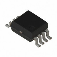
IC VIDEO AMP DIFF 8-SSOP
Manufacturer
NEC
Datasheet
1.UPC1663GV-E1-A.pdf
(5 pages)
Specifications of UPC1663GV-A
Applications
Differential
Output Type
Differential
Number Of Circuits
1
-3db Bandwidth
700MHz
Current - Supply
13mA
Current - Output / Channel
20mA
Mounting Type
Surface Mount
Package / Case
8-SSOP
Lead Free Status / RoHS Status
Lead free / RoHS Compliant


Notes:
1. Each lead centerline is located within 0.12 mm (0.005 inch)
2. All dimensions are typical unless otherwise specified.
OUTLINE DIMENSIONS
PIN DESCRIPTION
Life Support Applications
These NEC products are not intended for use in life support devices, appliances, or systems where the malfunction of these products can reasonably
be expected to result in personal injury. The customers of CEL using or selling these products for use in such applications do so at their own risk and
agree to fully indemnify CEL for all damages resulting from such improper use or sale.
of its true position at maximum material condition.
No.
Pin
8
1
5
4
6
3
7
2
1.8 MAX
DATA SUBJECT TO CHANGE WITHOUT NOTICE
CALIFORNIA EASTERN LABORATORIES • Headquarters • 4590 Patrick Henry Drive • Santa Clara, CA 95054-1817 • (408) 988-3500 • Telex 34-6393 • FAX (408) 988-0279
0.1 ± 0.1
1.5±0.1
8
1
N
EXCLUSIVE NORTH AMERICAN AGENT FOR
Name
1663
OUT
OUT
0.3
V
V
G
G
Pin
IN
IN
3.0 MAX
7
2
+0.10
CC
CC
-0.05
1A
1B
0.65
PACKAGE OUTLINE S08
1
2
+
-
1
2
6
3
0.575 MAX
5
4
UPC1663GV
0.15
±2 to ±6.5
voltage
voltage
In single
+0.10
-0.05
Pin
Pin
Bias
—
24-Hour Fax-On-Demand: 800-390-3232 (U.S. and Canada only) • Internet: http://WWW.CEL.COM
0
0
(V)
(Units in mm)
0.5 ± 0.2
Detail of Lead End
4.94 ± 0.2
-0.3 to +14
3.2±0.1
In single
voltage
voltage
Apply
V
Apply
V
GND
3
bias
+7˚
CC
CC
-3˚
—
(V)
/2
/2
0.87±0.2
Input pin
Output pin
Plus voltage supply pin.
This pin should be
connected with bypass
capacitor to minimize AC
impedance.
Minus voltage supply pin.
This pin should be
connected with bypass
capacitor to minimize AC
impedance.
Gain adjustment pin.
External resistor from 0 to
10 kW can be inserted
between pin 2 and 7 to
determine gain value.
Functions and Applications
RF, MICROWAVE & OPTOELECTRONIC SEMICONDUCTORS
CONNECTION DIAGRAM
ORDERING INFORMATION
UPC1663GV-E1-A
PART NUMBER
OUT
G
V
IN
Internal circuit constants should be refered to ap-
plication note.
1A
8
CC
2
2
7
-
4
2
3
1
UPC1663GV
Internal Equivalent Circuit
2
1
(TOP VIEW)
6
3
QUANTITY
1000/Reel
7
6
5
8
IN
G
V
OUT
CC
1B
11/04/2008
1
+
1
4
5
Related parts for UPC1663GV-A
Image
Part Number
Description
Manufacturer
Datasheet
Request
R

Part Number:
Description:
UPC1663DC to VHF WIDEBAND DIFFERENTIAL INPUT AND OUTPUT AMPLIFIER IC
Manufacturer:
NEC
Datasheet:
Part Number:
Description:
16/8 bit single-chip microcomputer
Manufacturer:
NEC
Datasheet:
Part Number:
Description:
Dual audio power amp circuit
Manufacturer:
NEC
Datasheet:
Part Number:
Description:
Dual comparator
Manufacturer:
NEC
Datasheet:
Part Number:
Description:
MOS type composite field effect transistor
Manufacturer:
NEC
Datasheet:
Part Number:
Description:
50 V/100 mA FET array incorporating 2 N-ch MOSFETs
Manufacturer:
NEC
Datasheet:
Part Number:
Description:
6-pin small MM high-frequency double transistor
Manufacturer:
NEC
Datasheet:
Part Number:
Description:
6-pin small MM high-frequency double transistor
Manufacturer:
NEC
Datasheet:
Part Number:
Description:
6-pin small MM high-frequency double transistor
Manufacturer:
NEC
Datasheet:
Part Number:
Description:
6-pin small MM high-frequency double transistor
Manufacturer:
NEC
Datasheet:
Part Number:
Description:
Twin transistors equipped with different model chips(6P small MM)
Manufacturer:
NEC
Datasheet: