BGD502,112 NXP Semiconductors, BGD502,112 Datasheet
BGD502,112
Specifications of BGD502,112


Related parts for BGD502,112


BGD502,112 Summary of contents
Page 1
DATA SHEET dbook, halfpage BGD502 550 MHz, 18.5 dB gain power doubler amplifier Product specification Supersedes data of 1995 Oct 25 DISCRETE SEMICONDUCTORS M3D252 2001 Nov 15 ...
Page 2
... NXP Semiconductors 550 MHz, 18.5 dB gain power doubler amplifier FEATURES Excellent linearity Extremely low noise Silicon nitride passivation Rugged construction TiPtAu metallized crystals ensure optimal reliability. DESCRIPTION Hybrid amplifier modules for CATV systems operating over a frequency range 550 MHz at a voltage supply (DC) ...
Page 3
... NXP Semiconductors 550 MHz, 18.5 dB gain power doubler amplifier CHARACTERISTICS Table 1 Bandwidth 40 to 550 MHz; V SYMBOL PARAMETER G power gain p SL slope cable equivalent FL flatness of frequency response s input return losses 11 s output return losses 22 s phase response 21 CTB composite triple beat X cross modulation ...
Page 4
... NXP Semiconductors 550 MHz, 18.5 dB gain power doubler amplifier Table 2 Bandwidth 40 to 450 MHz; V SYMBOL PARAMETER G power gain p SL slope cable equivalent FL flatness of frequency response s input return losses 11 s output return losses 22 s phase response 21 CTB composite triple beat CSO composite second order distortion ...
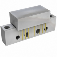
Page 5
... NXP Semiconductors 550 MHz, 18.5 dB gain power doubler amplifier PACKAGE OUTLINE Rectangular single-ended package; aluminium flange; 2 vertical mounting holes 6-32 UNC and 2 extra horizontal mounting holes; 7 gold-plated in-line leads DIMENSIONS (mm are the original dimensions UNIT b c max. max. max. 0.51 mm 20.8 9 ...
Page 6
... In no event shall NXP Semiconductors be liable for any indirect, incidental, punitive, special or consequential damages (including - without limitation - lost profits, lost savings, business interruption, costs related to the ...
Page 7
... NXP Semiconductors’ specifications such use shall be solely at customer’s own risk, and (c) customer fully indemnifies NXP Semiconductors for any liability, damages or failed product claims resulting from customer design and use of the product for automotive applications beyond NXP Semiconductors’ ...
Page 8
... Interface, Security and Digital Processing expertise Customer notification This data sheet was changed to reflect the new company name NXP Semiconductors, including new legal definitions and disclaimers. No changes were made to the technical content, except for package outline drawings which were updated to the latest version. ...