CS8416-CNZ Cirrus Logic Inc, CS8416-CNZ Datasheet - Page 5
CS8416-CNZ
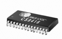
Manufacturer Part Number
CS8416-CNZ
Description
IC RCVR DGTL 192KHZ 28QFN COMM
Manufacturer
Cirrus Logic Inc
Type
Digital Audio Interface Receiverr
Datasheet
1.CS8416-CZZ.pdf
(60 pages)
Specifications of CS8416-CNZ
Applications
Digital Audio
Mounting Type
Surface Mount
Package / Case
28-QFN
Audio Control Type
Digital
Control Interface
I2C, SPI
Control / Process Application
AV & DVD Receivers, CD-R, Digital Mixing Consoles
Supply Voltage Range
3.13V To 5.25V, 3.13V To 3.46V
Lead Free Status / RoHS Status
Lead free / RoHS Compliant
For Use With
598-1017 - BOARD EVAL FOR CS8416 RCVR
Lead Free Status / RoHS Status
Lead free / RoHS Compliant, Lead free / RoHS Compliant
Other names
598-1723


DS578F3
LIST OF FIGURES
LIST OF TABLES
Figure 1. Audio Port Master Mode Timing ................................................................................................... 9
Figure 2. Audio Port Slave Mode and Data Input Timing............................................................................. 9
Figure 3. SPI Mode Timing ........................................................................................................................ 10
Figure 4. I²C Mode Timing ......................................................................................................................... 11
Figure 5. Typical Connection Diagram - Software Mode ........................................................................... 20
Figure 6. Typical Connection Diagram - Hardware Mode .......................................................................... 21
Figure 7. Serial Audio Output Example Formats........................................................................................ 24
Figure 8. AES3 Data Format...................................................................................................................... 25
Figure 9. Receiver Input Structure ............................................................................................................. 27
Figure 10. C/U Data Outputs...................................................................................................................... 32
Figure 11. Control Port Timing in SPI Mode .............................................................................................. 33
Figure 12. Control Port Timing, I²C Slave Mode Write............................................................................... 34
Figure 13. Control Port Timing, I²C Slave Mode Read............................................................................... 34
Figure 14. De-Emphasis Filter Response .................................................................................................. 39
Figure 15. Hardware Mode Data Flow ....................................................................................................... 46
Figure 16. Professional Input Circuit .......................................................................................................... 49
Figure 17. Transformerless Professional Input Circuit ............................................................................... 49
Figure 18. Consumer Input Circuit ............................................................................................................. 50
Figure 19. S/PDIF MUX Input Circuit ......................................................................................................... 50
Figure 20. TTL/CMOS Input Circuit............................................................................................................ 50
Figure 21. Channel Status Data Buffer Structure....................................................................................... 52
Figure 22. Flowchart for Reading the E Buffer........................................................................................... 52
Figure 23. PLL Block Diagram ................................................................................................................... 53
Figure 24. Recommended Layout Example............................................................................................... 54
Figure 25. Jitter Attenuation Characteristics of PLL................................................................................... 55
Table 1. Typical Delays by Frequency Values ........................................................................................... 26
Table 2. Clock Switching Output Clock Rates............................................................................................ 28
Table 3. GPO Pin Configurations............................................................................................................... 29
Table 4. Hardware Mode Start-Up Pin Conditions ..................................................................................... 47
Table 5. Hardware Mode Serial Audio Format Select................................................................................ 48
Table 6. External PLL Component Values ................................................................................................. 54
CS8416
5
Related parts for CS8416-CNZ
Image
Part Number
Description
Manufacturer
Datasheet
Request
R

Part Number:
Description:
IC RCVR DGTL 192KHZ 28TSSOP COMM
Manufacturer:
Cirrus Logic Inc
Datasheet:
Part Number:
Description:
IC RCVR DGTL 192KHZ 28SOIC COMM
Manufacturer:
Cirrus Logic Inc
Datasheet:

Part Number:
Description:
IC RCVR DGTL 192KHZ 28TSSOP AUTO
Manufacturer:
Cirrus Logic Inc
Datasheet:

Part Number:
Description:
IC, DIGITAL AUDIO RECEIVER, SOIC-28
Manufacturer:
Cirrus Logic Inc
Datasheet:

Part Number:
Description:
IC,Digital Audio Receiver,CMOS,LLCC,28PIN,PLASTIC
Manufacturer:
Cirrus Logic Inc
Datasheet:
Part Number:
Description:
IC,Digital Audio Receiver,CMOS,TSSOP,28PIN,PLASTIC
Manufacturer:
Cirrus Logic Inc
Datasheet:
Part Number:
Description:
IC,Digital Audio Receiver,CMOS,SOP,28PIN,PLASTIC
Manufacturer:
Cirrus Logic Inc
Datasheet:
Part Number:
Description:
IC,Digital Audio Receiver,CMOS,TSSOP,28PIN,PLASTIC
Manufacturer:
Cirrus Logic Inc
Datasheet:

Part Number:
Description:
Audio DSPs IC 192 kHz Digital Audio Receiver
Manufacturer:
Cirrus Logic Inc
Datasheet:
Part Number:
Description:
192 KHZ INDUSTRIAL DIGITAL AUDIO RECEIVER
Manufacturer:
Cirrus Logic Inc
Part Number:
Description:
IC,Digital Audio Receiver,CMOS,LLCC,28PIN,PLASTIC
Manufacturer:
Cirrus Logic Inc
Part Number:
Description:
Audio DSPs IC 192 kHz Digital Audio Receiver
Manufacturer:
Cirrus Logic Inc
Datasheet:

Part Number:
Description:
Development Kit
Manufacturer:
Cirrus Logic Inc
Datasheet: