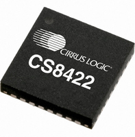
CS8422-CNZ Cirrus Logic Inc, CS8422-CNZ Datasheet - Page 11

CS8422-CNZ
Manufacturer Part Number
CS8422-CNZ
Description
IC SAMPLE RATE CONVERTER 32QFN
Manufacturer
Cirrus Logic Inc
Type
Sample Rate Converterr
Datasheet
1.CS8422-CNZ.pdf
(82 pages)
Specifications of CS8422-CNZ
Package / Case
32-QFN
Applications
Digital Audio
Mounting Type
Surface Mount
Maximum Operating Temperature
+ 125 C
Minimum Operating Temperature
- 55 C
Mounting Style
SMD/SMT
Package
32QFN
Operating Temperature
-55 to 125 °C
Audio Control Type
Sample Rate Converter
Control Interface
I2C, SPI
Supply Voltage Range
1.71V To 5.25V
Operating Temperature Range
-40°C To +85°C
Audio Ic Case Style
QFN
No. Of Pins
32
Rohs Compliant
Yes
Lead Free Status / RoHS Status
Lead free / RoHS Compliant
For Use With
598-1568 - BOARD EVAL FOR CS8422 RCVR
Lead Free Status / Rohs Status
Lead free / RoHS Compliant
Other names
598-1732
Available stocks
Company
Part Number
Manufacturer
Quantity
Price
Company:
Part Number:
CS8422-CNZ
Manufacturer:
CIRRUS
Quantity:
99
Part Number:
CS8422-CNZ
Manufacturer:
CIRRUS
Quantity:
20 000
Part Number:
CS8422-CNZR
Manufacturer:
CIRRUS
Quantity:
20 000
DS692F1
1.2
RXP/RXN[1:0]
VA
AGND
SAOF
MS_SEL
NV/RERR
V/AUDIO
XTI
XTO
Pin Name
Hardware Mode
Pin #
10
11
12
1
2
5
6
3
4
7
8
9
AES3/SPDIF Input (Input) - Differential receiver inputs carrying AES3 or S/PDIF encoded digital
data. RXP[1:0] comprise the non-inverting inputs of the differential input multiplexer; and RXN[1:0]
comprise the inverting inputs of the input multiplexer. Unused inputs should be tied to AGND.
Analog Power (Input) - Analog power supply, nominally +3.3 V. Care should be taken to ensure that
this supply is as noise-free as possible, as noise on this pin will directly affect the jitter performance of
the recovered clock.
Analog Ground (Input) - Ground for the analog circuitry in the chip. AGND and DGND should be
connected to a common ground area under the chip.
Serial Audio Output Format Select (Input) - Used to select the serial audio output format after RST
is released. See
Master/Slave Select (Input) - Used to select Master or Slave settings for the output serial audio ports
after RST is released. See
Non-Validity Receiver Error/Receiver Error (Output) - Receiver error indicator. NVERR is output by
default, RERR is selected by a 20 k resistor to VL.
Validity Data/AUDIO (Output) - If a 20 k pull-down is present on this pin, it will output serial Validity
data from the AES3 receiver, clocked by the rising and falling edges of OLRCK2 in master mode. If a
20 k pull-up is present, the pin will be low when valid linear PCM data is present at the AES3 input.
Crystal/Oscillator In (Input) - Crystal or digital clock input for Master clock. See
on page
Crystal Out (Output) - Crystal output for Master clock. See
MS_SEL
AGND
SAOF
RXN0
RXN1
RXP0
RXP1
38.
VA
1
2
3
4
5
6
7
8
Table 4 on page 41
32
9
10
31
Table 5 on page 41
11
30
32-Pin QFN Package
Thermal Pad
Top-Down View
29
12
for format settings.
13
28
Pin Description
14
27
for format settings.
15
26
25
16
“SRC Master Clock” on page
18
24
23
22
21
20
19
17
OSCLK2
SDOUT2
VL
DGND
VD_FILT
V_REG
TX/U
C
“SRC Master Clock”
CS8422
38.
11


