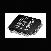
LPC11U24FBD64 NXP Semiconductors, LPC11U24FBD64 Datasheet - Page 32

LPC11U24FBD64
Manufacturer Part Number
LPC11U24FBD64
Description
The LPC11U24FBD64 is a ARM Cortex-M0 based, low-cost 32-bit MCU, designed for 8/16-bit microcontroller applications, offering performance, low power, simple instruction set and memory addressing together with reduced code size compared to existing 8/
Manufacturer
NXP Semiconductors
Datasheet
1.LPC11U23FBD48.pdf
(70 pages)
Available stocks
Company
Part Number
Manufacturer
Quantity
Price
Company:
Part Number:
LPC11U24FBD64/201
Manufacturer:
TOSHIBA
Quantity:
2 470
Company:
Part Number:
LPC11U24FBD64/401
Manufacturer:
NXP Semiconductors
Quantity:
10 000
Part Number:
LPC11U24FBD64/401
Manufacturer:
NXP/恩智浦
Quantity:
20 000
Company:
Part Number:
LPC11U24FBD64/401,
Manufacturer:
NXP Semiconductors
Quantity:
10 000
NXP Semiconductors
Table 5.
T
[1]
[3]
[4]
LPC11U2X
Product data sheet
[2]
[5]
[6]
Symbol Parameter
I
V
V
V
I
I
I
Oscillator pins
V
V
USB pins
I
V
V
V
V
V
V
C
Z
2
OL
OL
LI
OZ
amb
DRV
IH
IL
hys
i(xtal)
o(xtal)
BUS
DI
CM
th(rs)se
OL
OH
C-bus pins (PIO0_4 and PIO0_5)
trans
Typical ratings are not guaranteed. The values listed are at room temperature (25 C), nominal supply voltages.
For USB operation 3.0 V V
IRC enabled; system oscillator disabled; system PLL disabled.
I
BOD disabled.
All peripherals disabled in the AHBCLKCTRL register. Peripheral clocks to USART, SSP0/1 disabled in the SYSCON block.
DD
=
measurements were performed with all pins configured as GPIO outputs driven LOW and pull-up resistors disabled.
40
HIGH-level input
voltage
LOW-level input voltage
hysteresis voltage
LOW-level output
current
LOW-level output
current
input leakage current
crystal input voltage
crystal output voltage
OFF-state output
current
bus supply voltage
differential input
sensitivity voltage
differential common
mode voltage range
single-ended receiver
switching threshold
voltage
LOW-level output
voltage
HIGH-level output
voltage
transceiver capacitance pin to GND
driver output
impedance for driver
which is not high-speed
capable
Static characteristics
C to +85
C, unless otherwise specified.
DD
3.6 V. Guaranteed by design.
…continued
Conditions
V
as standard mode pins
V
as Fast-mode Plus pins
V
V
0 V < V
(D+) (D)
includes V
for low-/full-speed;
R
driven; for low-/full-speed;
R
with 33 series resistor; steady state
drive
OL
OL
I
I
L
L
2.0 V V
1.8 V V
2.0 V V
1.8 V V
= V
= 5 V
of 1.5 k to 3.6 V
of 15 k to GND
= 0.4 V; I
= 0.4 V; I
DD
All information provided in this document is subject to legal disclaimers.
I
< 3.3 V
DI
DD
DD
DD
DD
range
2
2
Rev. 2 — 13 January 2012
C-bus pins configured
C-bus pins configured
3.6 V
3.6 V
< 2.0 V
< 2.0 V
[16][2]
[15]
32-bit ARM Cortex-M0 microcontroller
[2]
[2]
[2]
[2]
[2]
[2]
[2]
[2]
Min
0.7V
-
-
3.5
3
20
16
-
-
0.5
0.5
-
-
0.2
0.8
0.8
-
2.8
-
36
DD
Typ
-
-
0.05V
-
-
-
-
2
10
1.8
1.8
-
-
-
-
-
-
-
-
-
[1]
LPC11U2x
DD
© NXP B.V. 2012. All rights reserved.
Max
-
-
-
-
4
22
1.95
1.95
10
5.25
-
2.5
2.0
0.18
3.5
20
0.3V
-
-
44.1
DD
32 of 70
Unit
V
V
V
mA
mA
A
A
V
V
A
V
V
V
V
V
V
pF


