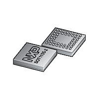
LPC11U24FET48 NXP Semiconductors, LPC11U24FET48 Datasheet - Page 14

LPC11U24FET48
Manufacturer Part Number
LPC11U24FET48
Description
The LPC11U24FET48 is a ARM Cortex-M0 based, low-cost 32-bit MCU, designed for 8/16-bit microcontroller applications, offering performance, low power, simple instruction set and memory addressing together with reduced code size compared to existing 8/
Manufacturer
NXP Semiconductors
Datasheet
1.LPC11U23FBD48.pdf
(70 pages)
Available stocks
Company
Part Number
Manufacturer
Quantity
Price
Company:
Part Number:
LPC11U24FET48/301,
Manufacturer:
NXP Semiconductors
Quantity:
10 000
NXP Semiconductors
Table 3.
[1]
[3]
[4]
[5]
[6]
[7]
[8]
7. Functional description
LPC11U2X
Product data sheet
[2]
Symbol
XTALOUT
V
V
DD
SS
Pin state at reset for default function: I = Input; O = Output; PU = internal pull-up enabled; IA = inactive, no pull-up/down enabled;
F = floating; If the pins are not used, tie floating pins to ground or power to minimize power consumption.
See
reset the chip and wake up from Deep power-down mode. An external pull-up resistor is required on this pin for the Deep power-down
mode.
5 V tolerant pad providing digital I/O functions with configurable pull-up/pull-down resistors and configurable hysteresis (see
I
5 V tolerant pad providing digital I/O functions with configurable pull-up/pull-down resistors and configurable hysteresis (see
includes high-current output driver.
5 V tolerant pad providing digital I/O functions with configurable pull-up/pull-down resistors, configurable hysteresis, and analog input.
When configured as a ADC input, digital section of the pad is disabled and the pin is not 5 V tolerant (see
input glitch filter.
Pad provides USB functions. It is designed in accordance with the USB specification, revision 2.0 (Full-speed and Low-speed mode
only). This pad is not 5 V tolerant.
When the system oscillator is not used, connect XTALIN and XTALOUT as follows: XTALIN can be left floating or can be grounded
(grounding is preferred to reduce susceptibility to noise). Leave XTALOUT floating.
2
C-bus pins compliant with the I
Figure 31
Pin description
for the reset pad configuration. RESET functionality is not available in Deep power-down mode. Use the WAKEUP pin to
7.1 On-chip flash programming memory
7.2 EEPROM
7.3 SRAM
7.4 On-chip ROM
The LPC11U2x contain 24 kB or 32 kB on-chip flash program memory. The flash can be
programmed using In-System Programming (ISP) or In-Application Programming (IAP)
via the on-chip boot loader software.
The LPC11U2x contain 1 kB, 2 kB, or 4 kB of on-chip byte-erasable and
byte-programmable EEPROM data memory. The EEPROM can be programmed using
In-Application Programming (IAP) via the on-chip boot loader software.
The LPC11U2x contain a total of 8 kB or 10 kB on-chip static RAM memory.
The on-chip ROM contains the boot loader and the following Application Programming
Interfaces (APIs):
5
6;
29
33
2
E1
B4;
E2
B5;
D2
C-bus specification for I
7
8;
44
5;
41
All information provided in this document is subject to legal disclaimers.
9
10;
33;
48;
58
7;
54
[8]
Rev. 2 — 13 January 2012
Reset
state
[1]
-
-
-
2
C standard mode, I
Type Description
-
-
-
Output from the oscillator amplifier.
Supply voltage to the internal regulator, the external
rail, and the ADC. Also used as the ADC reference
voltage.
Ground.
2
C Fast-mode, and I
32-bit ARM Cortex-M0 microcontroller
2
C Fast-mode Plus.
Figure
LPC11U2x
© NXP B.V. 2012. All rights reserved.
30); includes digital
Figure
Figure
14 of 70
30);
30).


