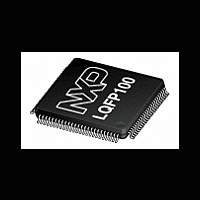
LPC2921_23_25 NXP Semiconductors, LPC2921_23_25 Datasheet - Page 18

LPC2921_23_25
Manufacturer Part Number
LPC2921_23_25
Description
The LPC2921/2923/2925 combine an ARM968E-S CPU core with two integrated TCMblocks operating at frequencies of up to 125 MHz, Full-speed USB 2
Manufacturer
NXP Semiconductors
Datasheet
1.LPC2921_23_25.pdf
(84 pages)
- Current page: 18 of 84
- Download datasheet (552Kb)
NXP Semiconductors
LPC2921_23_25_3
Product data sheet
6.8.2 Flash layout
With dual buffering, a secondary buffer line is used, the output of the flash being
considered as the primary buffer. On a primary buffer, hit data can be copied to the
secondary buffer line, which allows the flash to start a speculative read of the next flash
word.
Both buffer lines are invalidated after:
The modes of operation are listed in
Table 9.
The ARM processor can program the flash for ISP (In-System Programming) through the
flash memory controller. Note that the flash always has to be programmed by ‘flash words’
of 128 bits (four 32-bit AHB bus words, hence 16 bytes).
The flash memory is organized into eight ‘small’ sectors of 8 kB each and up to 11 ‘large’
sectors of 64 kB each. The number of large sectors depends on the device type. A sector
must be erased before data can be written to it. The flash memory also has sector-wise
protection. Writing occurs per page which consists of 4096 bits (32 flash words). A small
sector contains 16 pages; a large sector contains 128 pages.
Table 10
Table 10.
Synchronous timing
No buffer line
Single buffer line
Asynchronous timing
No buffer line
Single buffer line
Dual buffer line, single
speculative
Dual buffer line, always
speculative
Flash memory
sector number
11
12
13
14
15
•
•
•
•
Initialization
Configuration-register access
Data-latch reading
Index-sector reading
gives an overview of the flash-sector base addresses.
Flash read modes
Flash sector overview
All information provided in this document is subject to legal disclaimers.
Sector size (kB)
8
8
8
8
8
Rev. 03 — 14 April 2010
for single (non-linear) reads; one flash-word read per word read
default mode of operation; most recently read flash word is kept until
another flash word is required
one flash-word read per word read
most recently read flash word is kept until another flash word is
required
on a buffer miss a flash read is done, followed by at most one
speculative read; optimized for execution of code with small loops
(less than eight words) from flash
most recently used flash word is copied into second buffer line; next
flash-word read is started; highest performance for linear reads
Flash memory
address
0x2000 0000
0x2000 2000
0x2000 4000
0x2000 6000
0x2000 8000
Table
ARM9 microcontroller with CAN, LIN, and USB
9.
LPC2921/2923/2925
LPC2921
yes
yes
yes
yes
yes
LPC2923 LPC2925
yes
yes
yes
yes
yes
© NXP B.V. 2010. All rights reserved.
yes
yes
yes
yes
yes
18 of 84
Related parts for LPC2921_23_25
Image
Part Number
Description
Manufacturer
Datasheet
Request
R
Part Number:
Description:
Arm9 Microcontroller With Can, Lin, And Usb Device
Manufacturer:
NXP Semiconductors
Datasheet:
Part Number:
Description:
(LPC2921 - LPC2925) ARM9 microcontroller
Manufacturer:
NXP Semiconductors
Datasheet:
Part Number:
Description:
NXP Semiconductors designed the LPC2420/2460 microcontroller around a 16-bit/32-bitARM7TDMI-S CPU core with real-time debug interfaces that include both JTAG andembedded trace
Manufacturer:
NXP Semiconductors
Datasheet:

Part Number:
Description:
NXP Semiconductors designed the LPC2458 microcontroller around a 16-bit/32-bitARM7TDMI-S CPU core with real-time debug interfaces that include both JTAG andembedded trace
Manufacturer:
NXP Semiconductors
Datasheet:
Part Number:
Description:
NXP Semiconductors designed the LPC2468 microcontroller around a 16-bit/32-bitARM7TDMI-S CPU core with real-time debug interfaces that include both JTAG andembedded trace
Manufacturer:
NXP Semiconductors
Datasheet:
Part Number:
Description:
NXP Semiconductors designed the LPC2470 microcontroller, powered by theARM7TDMI-S core, to be a highly integrated microcontroller for a wide range ofapplications that require advanced communications and high quality graphic displays
Manufacturer:
NXP Semiconductors
Datasheet:
Part Number:
Description:
NXP Semiconductors designed the LPC2478 microcontroller, powered by theARM7TDMI-S core, to be a highly integrated microcontroller for a wide range ofapplications that require advanced communications and high quality graphic displays
Manufacturer:
NXP Semiconductors
Datasheet:
Part Number:
Description:
The Philips Semiconductors XA (eXtended Architecture) family of 16-bit single-chip microcontrollers is powerful enough to easily handle the requirements of high performance embedded applications, yet inexpensive enough to compete in the market for hi
Manufacturer:
NXP Semiconductors
Datasheet:
Part Number:
Description:
The XA-S3 device is a member of Philips Semiconductors? XA(eXtended Architecture) family of high performance 16-bitsingle-chip microcontrollers
Manufacturer:
NXP Semiconductors
Datasheet:

Part Number:
Description:
The NXP BlueStreak LH75401/LH75411 family consists of two low-cost 16/32-bit System-on-Chip (SoC) devices
Manufacturer:
NXP Semiconductors
Datasheet:

Part Number:
Description:
The NXP LPC3130/3131 combine an 180 MHz ARM926EJ-S CPU core, high-speed USB2
Manufacturer:
NXP Semiconductors
Datasheet:

Part Number:
Description:
The NXP LPC3141 combine a 270 MHz ARM926EJ-S CPU core, High-speed USB 2
Manufacturer:
NXP Semiconductors

Part Number:
Description:
The NXP LPC3143 combine a 270 MHz ARM926EJ-S CPU core, High-speed USB 2
Manufacturer:
NXP Semiconductors

Part Number:
Description:
The NXP LPC3152 combines an 180 MHz ARM926EJ-S CPU core, High-speed USB 2
Manufacturer:
NXP Semiconductors


