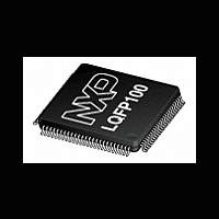
LPC2921_23_25 NXP Semiconductors, LPC2921_23_25 Datasheet - Page 27

LPC2921_23_25
Manufacturer Part Number
LPC2921_23_25
Description
The LPC2921/2923/2925 combine an ARM968E-S CPU core with two integrated TCMblocks operating at frequencies of up to 125 MHz, Full-speed USB 2
Manufacturer
NXP Semiconductors
Datasheet
1.LPC2921_23_25.pdf
(84 pages)
- Current page: 27 of 84
- Download datasheet (552Kb)
NXP Semiconductors
LPC2921_23_25_3
Product data sheet
6.12.5.1 Functional description
6.12.5.2 Pin description
The SPI module can operate in:
The SPI module is a master or slave interface for synchronous serial communication with
peripheral devices that have either Motorola SPI or Texas Instruments Synchronous
Serial Interfaces.
The SPI module performs serial-to-parallel conversion on data received from a peripheral
device. The transmit and receive paths are buffered with FIFO memories
(16 bits wide × 32 words deep). Serial data is transmitted on pins SDOx and received on
pins SDIx.
The SPI module includes a programmable bit-rate clock divider and prescaler to generate
the SPI serial clock from the input clock CLK_SPIx.
The SPI module’s operating mode, frame format, and word size are programmed through
the SLVn_SETTINGS registers.
A single combined interrupt request SPI_INTREQ output is asserted if any of the
interrupts are asserted and unmasked.
Depending on the operating mode selected, the SPI SCS outputs operate as an
active-HIGH frame synchronization output for Texas Instruments synchronous serial
frame format or an active-LOW chip select for SPI.
Each data frame is between four and 16 bits long, depending on the size of words
programmed, and is transmitted starting with the MSB.
The SPI pins are combined with other functions on the port pins of the
LPC2921/2923/2925, see
y runs from 0 to 3).
Table 15.
[1]
[2]
Symbol
SPIx SCSy
SPIx SCK
SPIx SDI
SPIx SDO
•
•
•
Internal loopback test mode.
Master mode:
– Normal transmission mode
– Sequential slave mode
Slave mode
Direction of SPIx SCS and SPIx SCK pins depends on master or slave mode. These pins are output in
master mode, input in slave mode.
In slave mode there is only one chip select input pin, SPIx SCS0. The other chip selects have no function in
slave mode.
SPI pins
SCSx[y]
SCKx
SDIx
SDOx
Pin name
All information provided in this document is subject to legal disclaimers.
Rev. 03 — 14 April 2010
Section
IN/OUT
IN
OUT
Direction
IN/OUT
6.11.3.
ARM9 microcontroller with CAN, LIN, and USB
SPIx data input
SPIx data output
Description
SPIx chip select
SPIx clock
Table 15
LPC2921/2923/2925
shows the SPI pins (x runs from 0 to 2;
[1]
[1][2]
© NXP B.V. 2010. All rights reserved.
27 of 84
Related parts for LPC2921_23_25
Image
Part Number
Description
Manufacturer
Datasheet
Request
R
Part Number:
Description:
Arm9 Microcontroller With Can, Lin, And Usb Device
Manufacturer:
NXP Semiconductors
Datasheet:
Part Number:
Description:
(LPC2921 - LPC2925) ARM9 microcontroller
Manufacturer:
NXP Semiconductors
Datasheet:
Part Number:
Description:
NXP Semiconductors designed the LPC2420/2460 microcontroller around a 16-bit/32-bitARM7TDMI-S CPU core with real-time debug interfaces that include both JTAG andembedded trace
Manufacturer:
NXP Semiconductors
Datasheet:

Part Number:
Description:
NXP Semiconductors designed the LPC2458 microcontroller around a 16-bit/32-bitARM7TDMI-S CPU core with real-time debug interfaces that include both JTAG andembedded trace
Manufacturer:
NXP Semiconductors
Datasheet:
Part Number:
Description:
NXP Semiconductors designed the LPC2468 microcontroller around a 16-bit/32-bitARM7TDMI-S CPU core with real-time debug interfaces that include both JTAG andembedded trace
Manufacturer:
NXP Semiconductors
Datasheet:
Part Number:
Description:
NXP Semiconductors designed the LPC2470 microcontroller, powered by theARM7TDMI-S core, to be a highly integrated microcontroller for a wide range ofapplications that require advanced communications and high quality graphic displays
Manufacturer:
NXP Semiconductors
Datasheet:
Part Number:
Description:
NXP Semiconductors designed the LPC2478 microcontroller, powered by theARM7TDMI-S core, to be a highly integrated microcontroller for a wide range ofapplications that require advanced communications and high quality graphic displays
Manufacturer:
NXP Semiconductors
Datasheet:
Part Number:
Description:
The Philips Semiconductors XA (eXtended Architecture) family of 16-bit single-chip microcontrollers is powerful enough to easily handle the requirements of high performance embedded applications, yet inexpensive enough to compete in the market for hi
Manufacturer:
NXP Semiconductors
Datasheet:
Part Number:
Description:
The XA-S3 device is a member of Philips Semiconductors? XA(eXtended Architecture) family of high performance 16-bitsingle-chip microcontrollers
Manufacturer:
NXP Semiconductors
Datasheet:

Part Number:
Description:
The NXP BlueStreak LH75401/LH75411 family consists of two low-cost 16/32-bit System-on-Chip (SoC) devices
Manufacturer:
NXP Semiconductors
Datasheet:

Part Number:
Description:
The NXP LPC3130/3131 combine an 180 MHz ARM926EJ-S CPU core, high-speed USB2
Manufacturer:
NXP Semiconductors
Datasheet:

Part Number:
Description:
The NXP LPC3141 combine a 270 MHz ARM926EJ-S CPU core, High-speed USB 2
Manufacturer:
NXP Semiconductors

Part Number:
Description:
The NXP LPC3143 combine a 270 MHz ARM926EJ-S CPU core, High-speed USB 2
Manufacturer:
NXP Semiconductors

Part Number:
Description:
The NXP LPC3152 combines an 180 MHz ARM926EJ-S CPU core, High-speed USB 2
Manufacturer:
NXP Semiconductors


