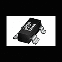
BF1118 NXP Semiconductors, BF1118 Datasheet

BF1118
Available stocks
Related parts for BF1118
BF1118 Summary of contents
Page 1
... General description These switches are a combination of a depletion type Field-Effect Transistor (FET) and a band-switching diode. The BF1118, BF1118R, BF1118W and BF1118WR are encapsulated in the SOT143B, SOT143R, SOT343N and SOT343R respectively. The low loss and high isolation capabilities of these devices provide excellent RF switching functions ...
Page 2
... Drain and source are interchangeable. 3. Ordering information Table 3. Type number Package BF1118 BF1118R BF1118W BF1118WR BF1118_1118R_1118W_1118WR Product data sheet BF1118(R); BF1118W(R) Pinning [1] [1] [1] [1] [1] [1] [1] [1] Ordering information Name Description - plastic surface-mounted package; 4 leads - plastic surface-mounted package; reverse pinning; 4 leads - plastic surface-mounted package ...
Page 3
... Thermal characteristics Table 6. Symbol R th(j-sp) [1] Soldering point of FET gate and diode anode lead. BF1118_1118R_1118W_1118WR Product data sheet BF1118(R); BF1118W(R) Marking Limiting values Parameter Conditions drain-source voltage source-drain voltage drain-gate voltage source-gate voltage drain current reverse voltage forward current storage temperature ...
Page 4
... MHz mA 100 MHz F and the series connection All information provided in this document is subject to legal disclaimers. Rev. 2 — 11 January 2012 BF1118(R); BF1118W(R) Silicon RF switches Min Typ = 0 A ...
Page 5
... (diode F Figure 3. Fig 2. V BF1118/BF1118R/ BF1118W/BF1118RW Ω input V All information provided in this document is subject to legal disclaimers. Rev. 2 — 11 January 2012 BF1118(R); BF1118W(R) 0 ISL off (dB) −20 −40 −60 0 200 400 600 = 50 3 ...
Page 6
... Plastic surface-mounted package; 4 leads DIMENSIONS (mm are the original dimensions UNIT max 1.1 0.48 0.88 0.1 mm 0.9 0.38 0.78 OUTLINE VERSION IEC SOT143B Fig 4. Package outline SOT143B BF1118_1118R_1118W_1118WR Product data sheet BF1118(R); BF1118W( scale 0.15 3.0 1.4 1.9 1.7 0.09 2.8 1 ...
Page 7
... Plastic surface-mounted package; reverse pinning; 4 leads DIMENSIONS (mm are the original dimensions UNIT max 1.1 0.48 0.88 0.1 mm 0.9 0.38 0.78 OUTLINE VERSION IEC SOT143R Fig 5. Package outline SOT143R BF1118_1118R_1118W_1118WR Product data sheet BF1118(R); BF1118W( scale 0.15 3.0 1.4 1.9 1.7 ...
Page 8
... Plastic surface-mounted package; 4 leads DIMENSIONS (mm are the original dimensions UNIT max 0.4 0.7 1.1 mm 0.1 0.8 0.3 0.5 OUTLINE VERSION IEC SOT343N Fig 6. Package outline SOT343N BF1118_1118R_1118W_1118WR Product data sheet BF1118(R); BF1118W( scale 0.25 2.2 1.35 1.3 1.15 0.10 1.8 1.15 REFERENCES ...
Page 9
... scale 0.25 2.2 1.35 1.3 1.15 0.10 1.8 1.15 REFERENCES JEDEC EIAJ All information provided in this document is subject to legal disclaimers. Rev. 2 — 11 January 2012 BF1118(R); BF1118W(R) Silicon RF switches detail 2.2 0.45 0.23 0.2 0.2 2.0 0.15 0.13 EUROPEAN PROJECTION ...
Page 10
... S4 VCR 11. Revision history Table 10. Revision history Document ID BF1118_1118R_1118W_1118WR v.2 Modifications: BF1118_1118R_1118W_1118WR v.1 BF1118_1118R_1118W_1118WR Product data sheet BF1118(R); BF1118W(R) Abbreviations Description Acceptable Quality Level Metal-Oxide Semiconductor Field-Effect Transistor Radio Frequency Special inspection level 4 Video Cassette Recorder Release date Data sheet status 20120111 Product data sheet • ...
Page 11
... This document supersedes and replaces all information supplied prior to the publication hereof. BF1118_1118R_1118W_1118WR Product data sheet BF1118(R); BF1118W(R) [3] Definition This document contains data from the objective specification for product development. This document contains data from the preliminary specification. ...
Page 12
... For sales office addresses, please send an email to: BF1118_1118R_1118W_1118WR Product data sheet BF1118(R); BF1118W(R) In the event that customer uses the product for design-in and use in automotive applications to automotive specifications and standards, customer (a) shall use the product without NXP Semiconductors’ warranty of the ...
Page 13
... Please be aware that important notices concerning this document and the product(s) described herein, have been included in section ‘Legal information’. © NXP B.V. 2012. For more information, please visit: http://www.nxp.com For sales office addresses, please send an email to: salesaddresses@nxp.com Document identifier: BF1118_1118R_1118W_1118WR Silicon RF switches All rights reserved. Date of release: 11 January 2012 ...


