ICS660GILF IDT, Integrated Device Technology Inc, ICS660GILF Datasheet - Page 3
ICS660GILF
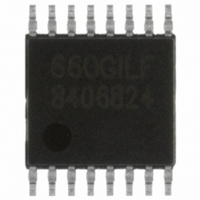
Manufacturer Part Number
ICS660GILF
Description
IC VIDEO CLK SOURCE DGTL 16TSSOP
Manufacturer
IDT, Integrated Device Technology Inc
Type
Clock Generatorr
Datasheet
1.ICS660GILF.pdf
(7 pages)
Specifications of ICS660GILF
Applications
Digital Video
Mounting Type
Surface Mount
Package / Case
16-TSSOP
Number Of Elements
1
Supply Current
25mA
Pll Input Freq (min)
13.5MHz
Pll Input Freq (max)
125MHz
Operating Supply Voltage (typ)
3.3V
Operating Temp Range
-40C to 85C
Package Type
TSSOP
Output Frequency Range
14.318 to 125MHz
Operating Supply Voltage (min)
3V
Operating Supply Voltage (max)
3.6V
Operating Temperature Classification
Industrial
Pin Count
16
Lead Free Status / RoHS Status
Lead free / RoHS Compliant
Other names
660GILF
800-1088
800-1088-5
800-1088
800-1088
800-1088-5
800-1088
Available stocks
Company
Part Number
Manufacturer
Quantity
Price

Part Number:
ICS660GILF
Manufacturer:
N/A
Quantity:
20 000


Application Information
Series Termination Resistor
Clock output traces should use series termination. To series
terminate a 50 trace (a commonly used trace impedance),
place a 33 resistor in series with the clock line, as close to
the clock output pin as possible. The nominal impedance of
the clock output is 20 .
Decoupling Capacitors
As with any high-performance mixed-signal IC, the ICS660
must be isolated from system power supply noise to perform
optimally.
Decoupling capacitors of 0.01µF must be connected
between each VDD and the PCB ground plane. To further
guard against interfering system supply noise, the ICS660
should use one common connection to the PCB power
plane as shown in the diagram on the next page. The ferrite
bead and bulk capacitor help reduce lower frequency noise
in the supply that can lead to output clock phase modulation.
Recommended Power Supply Connection for
All power supply pins must be connected to the same
voltage, except VDDR and VDDO, which may be connected
to a lower voltage in order to change the output level. If the
reference output is not used, ground VDDR.
Crystal Load Capacitors
If a crystal is used, the device crystal connections should
include pads for capacitors from X1 to ground and from X2
to ground. These capacitors are used to adjust the stray
IDT™ / ICS™ DIGITAL VIDEO CLOCK SOURCE
ICS660
DIGITAL VIDEO CLOCK SOURCE
B ulk D ecoupling C apacitor
C onnection to 3.3V
(such as 1 F Tantalum )
Optimal Device Performance
0.01
P ow er P lane
F D ecoupling C apacitors
Ferrite
Bead
V D D P in
V D D P in
V D D P in
3
capacitance of the board to match the nominally required
crystal load capacitance. To reduce possible noise pickup,
use very short PCB traces (and no vias) been the crystal
and device.
The value of the load capacitors can be roughly determined
by the formula C = 2(C
connected to X1 and X2, and C
load capacitance for the crystal. A typical crystal C
so C = 2(18 - 6) = 24 pF. Because these capacitors adjust
the stray capacitance of the PCB, check the output
frequency using your final layout to see if the value of C
should be changed.
PCB Layout Recommendations
For optimum device performance and lowest output phase
noise, the following guidelines should be observed.
1) Each 0.01µF decoupling capacitor should be mounted on
the component side of the board as close to the VDD pin as
possible. No vias should be used between decoupling
capacitor and VDD pin. The PCB trace to VDD pin should
be kept as short as possible, as should the PCB trace to the
ground via. Distance of the ferrite bead and bulk decoupling
from the device is less critical.
2) The external crystal should be mounted next to the device
with short traces. The X1 and X2 traces should not be
routed next to each other with minimum spaces, instead
they should be separated and away from other traces.
3) To minimize EMI, and obtain the best signal integrity, the
33 series termination resistor should be placed close to
the clock output.
4) An optimum layout is one with all components on the
same side of the board, minimizing vias through other signal
layers (the ferrite bead and bulk decoupling capacitor can be
mounted on the back). Other signal traces should be routed
away from the ICS660. This includes signal traces just
underneath the device, or on layers adjacent to the ground
plane layer used by the device.
L
- 6) where C is the load capacitor
L
is the specified value of the
ICS660
CLOCK SYNTHESIZER
REV G 051310
L
is 18 pF,
Related parts for ICS660GILF
Image
Part Number
Description
Manufacturer
Datasheet
Request
R

Part Number:
Description:
TRANSLATION DEVICE DPI 80-PQFP
Manufacturer:
IDT, Integrated Device Technology Inc
Datasheet:
Part Number:
Description:
IDT PART
Manufacturer:
IDT, Integrated Device Technology Inc
Datasheet:
Part Number:
Description:
IC LIU T1/E1/J1 OCTAL 256PBGA
Manufacturer:
IDT, Integrated Device Technology Inc
Datasheet:

Part Number:
Description:
IC FREQ TIMING GENERATOR 28TSSOP
Manufacturer:
IDT, Integrated Device Technology Inc
Datasheet:
Part Number:
Description:
IC CLK DVR PLL 1:10 40VFQFPN
Manufacturer:
IDT, Integrated Device Technology Inc
Datasheet:
Part Number:
Description:
IC CLK FANOUT BUFFER 1:18 32LQFP
Manufacturer:
IDT, Integrated Device Technology Inc
Datasheet:
Part Number:
Description:
IC CLK FANOUT BUFFER 1:18 32LQFP
Manufacturer:
IDT, Integrated Device Technology Inc
Datasheet:
Part Number:
Description:
IC CK505 VREG/RES 56TSSOP
Manufacturer:
IDT, Integrated Device Technology Inc
Datasheet:

Part Number:
Description:
IC SDRAM CLK DVR 1:10 48-TSSOP
Manufacturer:
IDT, Integrated Device Technology Inc
Datasheet:

Part Number:
Description:
IC CLK DVR PLL 1:10 48TSSOP
Manufacturer:
IDT, Integrated Device Technology Inc
Datasheet:
Part Number:
Description:
IC FLEXPC CLK PROGR P4 56-TSSOP
Manufacturer:
IDT, Integrated Device Technology Inc
Datasheet:
Part Number:
Description:
IC FLEXPC CLK PROGR P4 56-TSSOP
Manufacturer:
IDT, Integrated Device Technology Inc
Datasheet:
Part Number:
Description:
IC FLEXPC CLK PROGR P4 56-SSOP
Manufacturer:
IDT, Integrated Device Technology Inc
Datasheet:

Part Number:
Description:
IC PLL CLK DRIVER 2.5V 28-TSSOP
Manufacturer:
IDT, Integrated Device Technology Inc
Datasheet:
Part Number:
Description:
IC CLOCK DRIVER 2.5V 24-TSSOP
Manufacturer:
IDT, Integrated Device Technology Inc
Datasheet: